Process for cutting wire net of silicon wafers

A cutting process and wire mesh technology, which is applied in the field of solar cell silicon wafer wire mesh cutting technology, can solve the problems of increasing the proportion of hidden cracks, missing corners and fragments, affecting the slicing efficiency, and disconnecting the cutting wire network. Fast and accurate mesh layout, improved wafer quality, and reduced line marks

Active Publication Date: 2011-06-15
TRINA SOLAR CO LTD
View PDF3 Cites 7 Cited by
  • Summary
  • Abstract
  • Description
  • Claims
  • Application Information

AI Technical Summary

Problems solved by technology

However, there is a fundamental technical difficulty in the wire mesh cutting process: when arranging the wire mesh, since the groove distance of the guide wheel grooves on the guide wheel is only about 0.36mm, it is difficult for the operator to ensure the same straight line of the wire mesh. It can be wound on the two guide wheel grooves that completely correspond to the two guide wheels. It is only based on the experience and feeling of the operator without any inspection and checking measures. If the same straight line cannot be wound on the two guide wheels that completely correspond to the two guide wheels On the wheel groove, the misalignment of the wires will lead to an increase in the proportion of hidden cracks, thick slices, line marks, missing corners and fragments during the slicing process, and even lead to the disconnection of the cutting wire network, which seriously affects the slicing efficiency

Method used


Image

  • Process for cutting wire net of silicon wafers
  • Process for cutting wire net of silicon wafers

Examples


Embodiment Construction

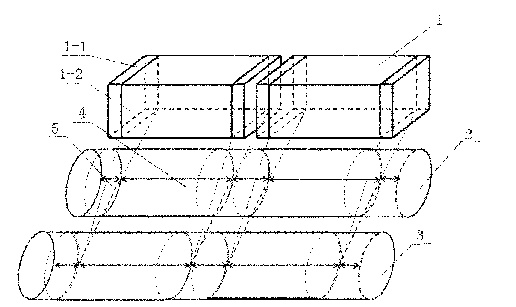
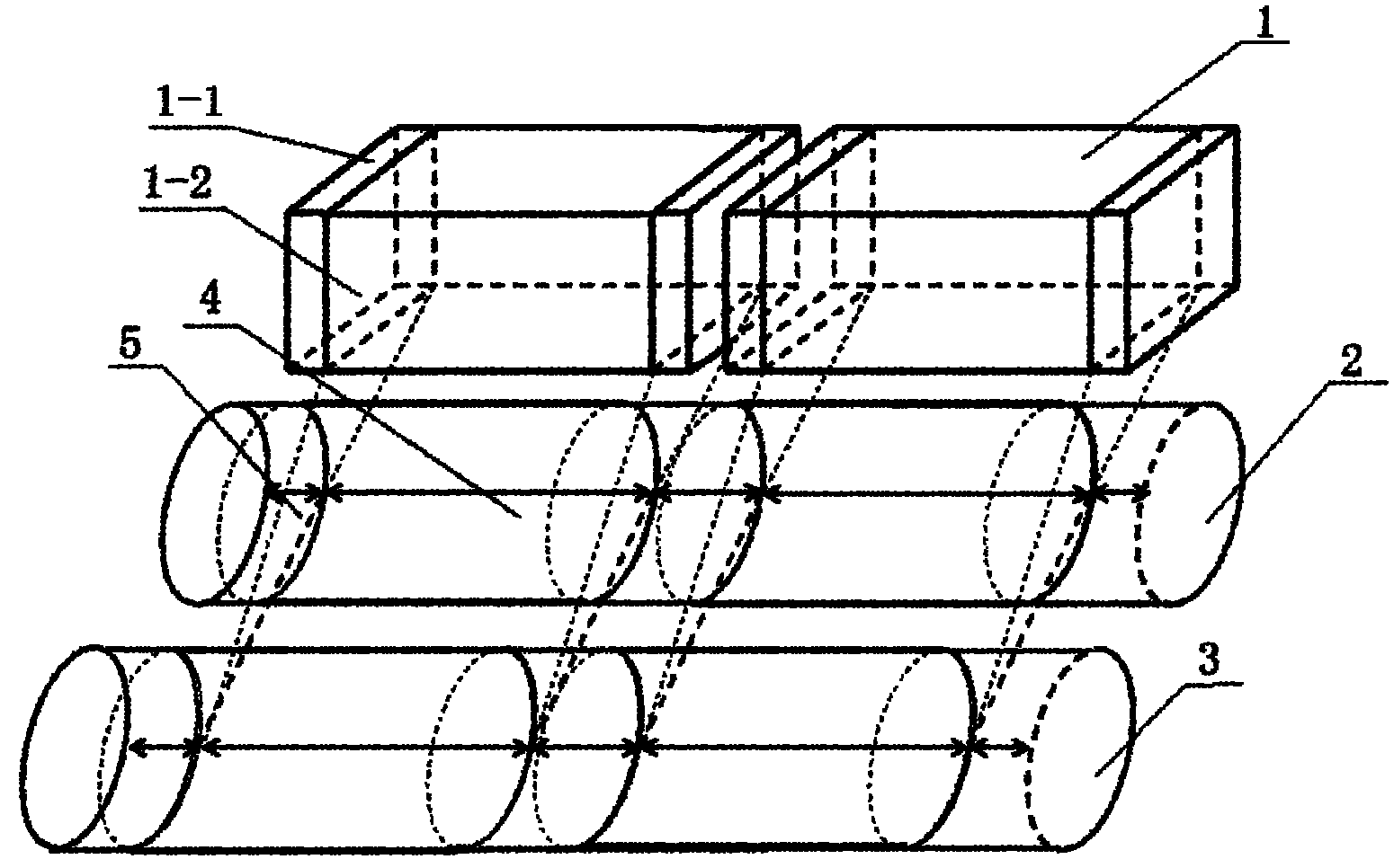
[0010] Such as figure 1 As shown, a silicon wafer wire mesh cutting process is used for slicing the crystal blocks for manufacturing solar cells, and has the following steps:

[0011] (1) First, mark the section 1-1 that does not need to be sliced ​​and the section 1-2 that needs to be sliced ​​for the ingot 1 that has not undergone the truncation process, and record the slice length and ingot length of the ingot 1 . The crystal ingot is squared, inspected, chamfered, and ground to form a crystal block 1 without truncation and truncation process, which saves the head and tail truncation process of the crystal block in the non-separation wire mesh cutting process. Put the crystal block 1 and auxiliary materials such as glass plates in an ultrasonic tank with a soft rubber pad and an appropriate amount of water; The plate is pasted in the center of the aluminum plate, and the glass and the aluminum plate are firmly adhered by the pressure method; the glue is evenly applied to t...


PUM


Abstract

The invention relates to a process for cutting a wire net of silicon wafers, which comprises the following steps of: marking a part to be cut and a part not to be cut on a wafer; marking parts to be slotted and parts not to be slotted for a first guide wheel and a second guide wheel, arranging guide wheel slots on the parts to be slotted of the first and the second guide wheels, when the wafer is installed on a cutting machine, and enabling the part to be cut of the wafer to correspond to the parts to be slotted of the first guide wheel and the second guide wheel, and the part of the wafer not to be cut to correspond to the parts not to be slotted of the first guide wheel and the second wheel. By redesigning the slotting mode of the guide wheels in the wire net cutting process, the process enables the arrangement of the wire net to be quick and accurate, completely avoids the defects of hidden cracked wafers, thick and thin wafers, scratch wafers, broken corner wafers and fragment wafers caused by displacement of steel wires on the two guide wheels in wiring, greatly improves the quality of the silicon wafer, and further provides guarantee for the yield of the silicon wafers at battery ends.

Description

technical field [0001] The invention relates to a process for cutting a solar battery silicon wafer dividing line net. Background technique [0002] At present, when slicing polycrystalline ingots of silicon wafers for solar cells at home and abroad, usually before the ingots enter the slicing machine for slicing, silicon wafer manufacturers need to cut off the ingots with band saws, inner circles or wires. The unqualified parts at both ends will increase the production process and production cost; at the same time, whether it is band saw truncation, inner circle truncation or line truncation, there will be slopes on the front and rear end faces of the crystal block, and some slopes will be generated during the silicon wafer cutting process. It will cause the steel to slip, scratch, etc. on the inclined surface, resulting in wire breakage, which will lead to more serious material loss and waste. [0003] Some companies use the split-line net cutting process of cutting off t...

Claims


Application Information

Patent Timeline
Patent Type & Authority Applications(China)
IPC IPC(8): B28D5/00
Inventor 贺洁
Owner TRINA SOLAR CO LTD
Why Eureka
Try Eureka