

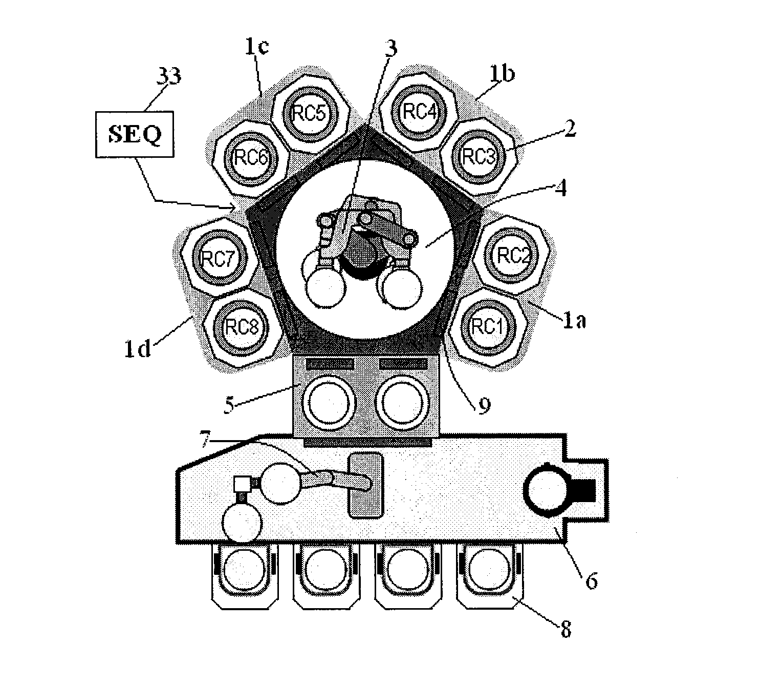
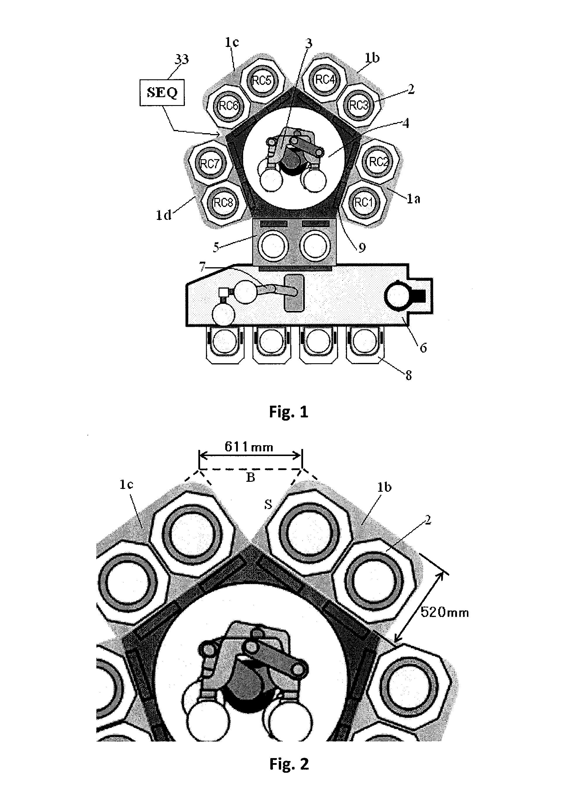
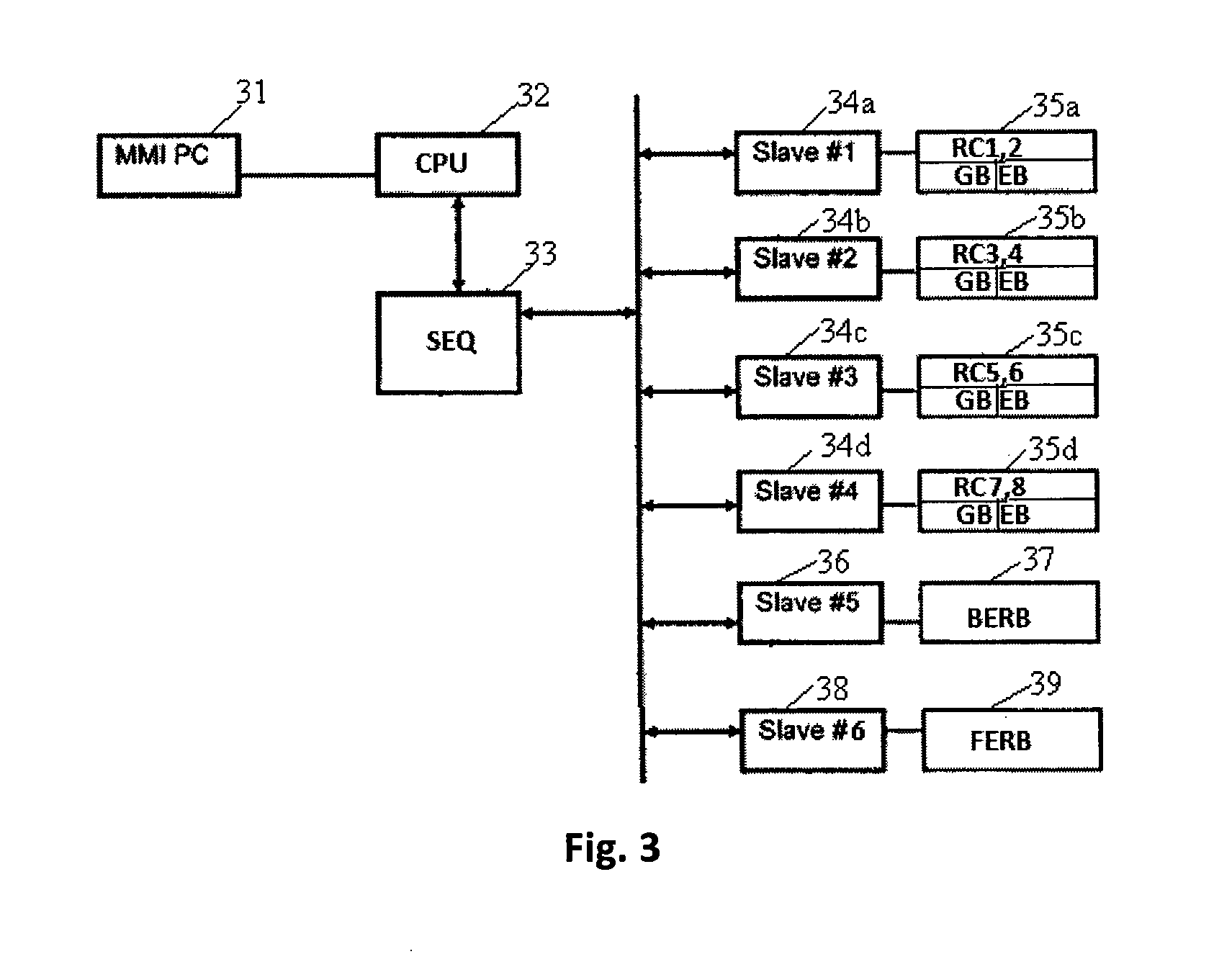
High-throughput semiconductor-processing apparatus equipped with multiple dual-chamber modules
a semiconductor processing and dual-chamber technology, applied in the direction of instrumentation, electric programme control, program control, etc., can solve the problems of wafer handling robots not fully and continuously operating, wafer handling time is getting close to its limit, and the operation of shorter tim
- Summary
- Abstract
- Description
- Claims
- Application Information
AI Technical Summary
Benefits of technology
Problems solved by technology
Method used
Image

Examples
Embodiment Construction
[0035]In this disclosure, “gas” may include vaporized solid and / or liquid and may be constituted by a mixture of gases. In this disclosure, the reactive gas, the additive gas, and the hydrogen-containing silicon precursor may be different from each other or mutually exclusive in terms of gas types, i.e., there is no overlap of gas types among these categories. Gases can be supplied in sequence with or without overlap.
[0036]In some embodiments, “film” refers to a layer continuously extending in a direction perpendicular to a thickness direction substantially without pinholes to cover an entire target or concerned surface, or simply a layer covering a target or concerned surface. In some embodiments, “layer” refers to a structure having a certain thickness formed on a surface or a synonym of film. A film or layer may be constituted by a discrete single film or layer having certain characteristics or multiple films or layers, and a boundary between adjacent films or layers may or may n...
PUM
| Property | Measurement | Unit |
|---|---|---|
| thickness | aaaaa | aaaaa |
| process time | aaaaa | aaaaa |
| process time | aaaaa | aaaaa |
Abstract
Description
Claims
Application Information