Source-clock-synchronized memory system and memory unit

a memory system and memory unit technology, applied in the direction of memory adressing/allocation/relocation, instruments, generating/distributing signals, etc., can solve the problems of limited memory capacity per memory bus (memory bank), limited number of memory modules that can be mounted on the memory riser board b0, and the number of pins for data signals is required. , to achieve the effect of large data storage capacity per memory and high mounting density

Inactive Publication Date: 2000-03-07
DELTA KOGYO CO LTD +1
View PDF14 Cites 533 Cited by
  • Summary
  • Abstract
  • Description
  • Claims
  • Application Information

AI Technical Summary

Benefits of technology

It is an object of the present invention to provide a source-clock-synchronized memory system having a large data st...

Problems solved by technology

As a result, the number of memory modules that can be mounted on the memory riser board B0 is also limited.
Therefore, the memory capacity per memory bus (memory bank) is limited due to restriction on the height of the memory riser board B0.
Since the memory controller 100 is connected to the input and output of the data line S3 which is a ring-type bus wired to the memory modules, there is raised a problem that a number of terminals (pins) for the data signal are required.
In such a conventional c...

Method used


Image

  • Source-clock-synchronized memory system and memory unit
  • Source-clock-synchronized memory system and memory unit
  • Source-clock-synchronized memory system and memory unit

Examples


first embodiment

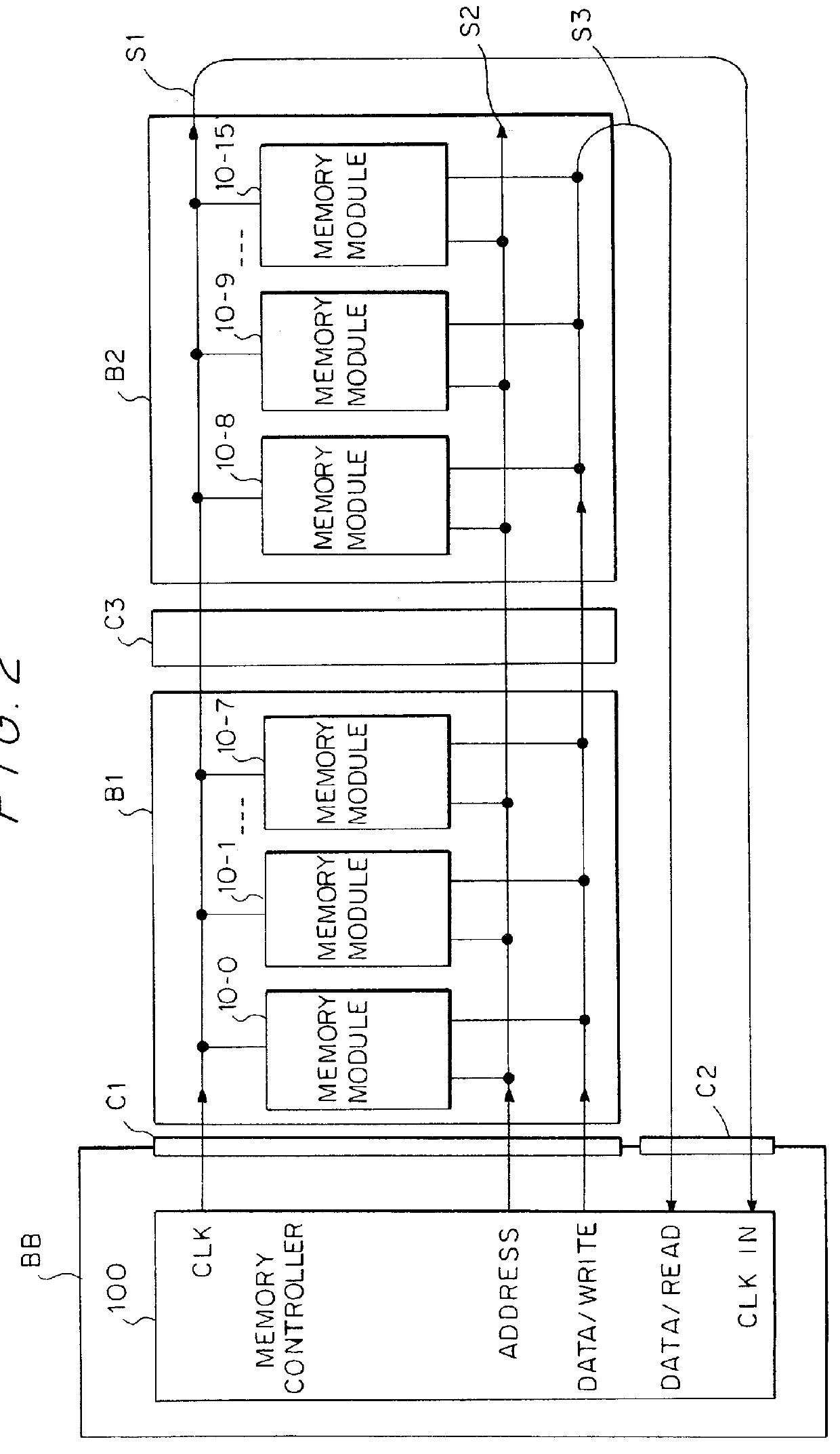
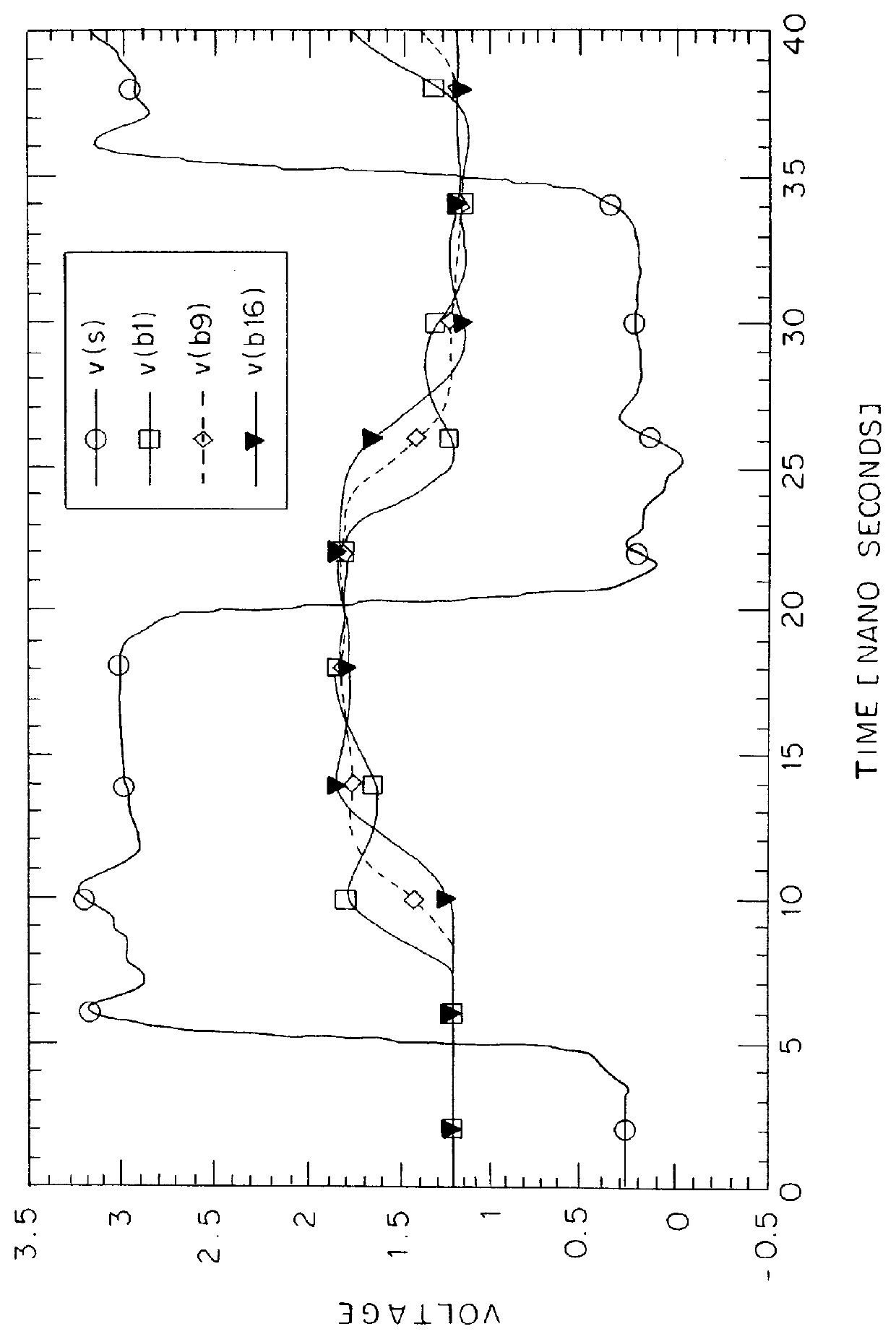
FIG. 3 is a diagram showing waveforms on the address bus resulting from SPICE simulation of the source-clock-synchronized system implemented by the first embodiment, wherein eight memory modules are mounted on each or the first and second memory riser boards B1 and B2 by adopting SSTL (Stub Series Terminated Logic) in the interface of the memory bus. FIG. 4 is a diagram showing a simulation circuit used in the simulation.

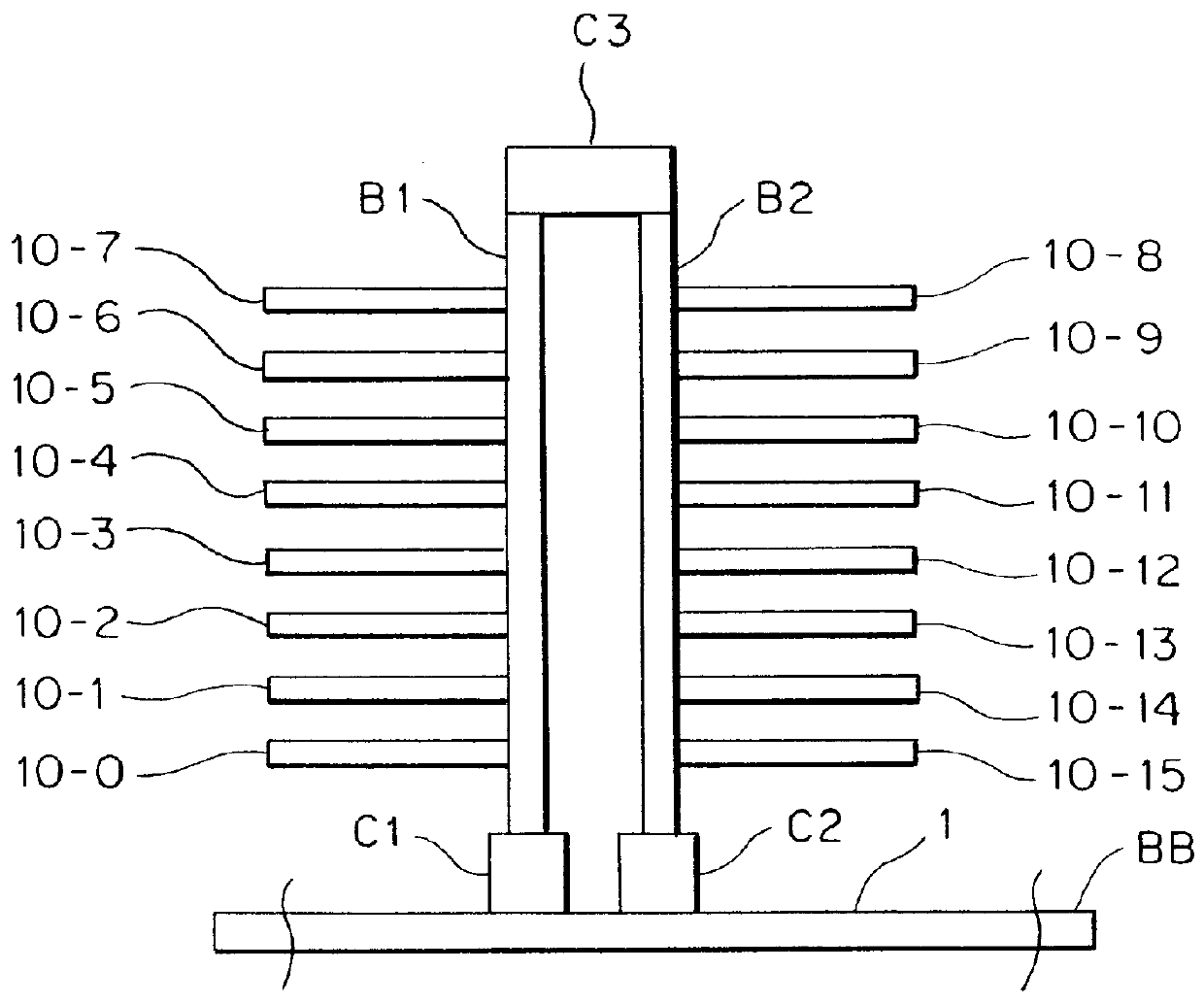
Points of observation for producing the waveforms shown in FIG. 3 are an output point (S) of the memory controller, a memory pin (b1) of the first memory module 10-0, a memory pin (b9) of the ninth memory module 10-8 and a memory pin (b16) of the sixteenth memory module 10-15. The waveforms observed at the points of observation S, b1, b9 and b16 are denoted by notations v(S), v(b1), v(b9) and v(b16) in FIG. 3 respectively. As may be obvious from the FIG. 3, the waveforms observed at the points of observation are stable. In addition, it is also known that the operati...

second embodiment

As shown in FIG. 6, the first and second connectors C1 and C2, the first and second memory riser boards B1 and B2 as well as the board linking connector C3 employed in the source-clock-synchronized memory system implemented by the present embodiment are the same as those of the In the memory controller 100, however, a data input / output common pin Data is used in place of the write-data output pin Data / Write and the read-data input pin Data / Read. In addition, on the base board BB, there is provided a switch SW0 for connecting the data input / output common pin Data to either the data line of the first connector C1 or the data line of the second connector C2. That is to say, the present embodiment is characterized in that the switch SW0 is switched in transitions from a write cycle to a read cycle or vice versa in accordance with a control signal generated by the memory controller 100. It should be noted that the control signal itself is not shown in the FIG. 6.

It is obvious that the s...

fourth embodiment

The following is description of a source-clock-synchronized memory system implemented by the present invention with reference to FIG. 7.

FIG. 7 is a block diagram showing the configuration of the source-clock-synchronized memory system implemented by the fourth embodiment. Components employed in the source-clock-synchronized memory system shown in FIG. 7 identical with those shown in FIGS. 2, 5 and 6 are denoted by the same reference numerals used in the latter. In addition, the external view of the source-clock-synchronized memory system implemented by the fourth embodiment is the same as that of the conventional source-clock-synchronized memory system shown in FIG. 21.

As shown in FIG. 7, the source-clock-synchronized memory system implemented by the fourth embodiment comprises a base board BB, a memory controller 100 provided on the base board BB, a connector C0 and a memory riser board B0. In the memory controller 100, a data input / output common pin Data is used in place of the wr...


PUM


Abstract

A source-clock-synchronized memory system having a large data storage capacity per memory bank and a high mounting density. The invention includes a memory unit having a first memory riser board B1 mounted on a base board through a first connector C1 and a second memory riser board B2 mounted on the base board BB through a second connector C2. The first memory riser board has a plurality of first memory modules mounted on the front surface thereof and the second memory riser board has a plurality of second memory modules mounted on the front surface thereof. The first and second memory riser boards are arranged in such a way that the back surface of the first memory riser board faces the back surface of the second memory riser board. The invention further includes a board linking connector for connecting signal lines on the first memory riser board to corresponding signal lines on the second memory riser board.

Description

BACKGROUND OF THE INVENTIONThe present invention relates to a technology for exchanging signals between a memory controller and a memory device employed in an information processing apparatus. More particularly, the present invention relates to a memory system for transmitting signals at a high speed to a plurality of memory devices connected to a common transmission line.In order to implement the IEEE P1596.4 (SyncLink), there has been proposed RamLink, a high-speed memory system employed in an information processing apparatus as disclosed in "SyncLink: A Proposal for an Implementation of IEEE P1596.4 `Ramlink` Optimized for Small (Single-Board) Memory System" by H. Wiggers, Hewlett Packard Company, which was published Mar. 23, 1995, pp 1-6. RamLink is a DRAM system for implementing a transfer speed equal to or higher than 500 Mbytes / s as a bandwidth. Five different topologies have been proposed. As a characteristic of a fourth option among the five proposed topologies, there is pr...

Claims


Application Information

Patent Timeline
IPC IPC(8): G06F12/06G06F12/00G06F1/10G06F13/16G11C13/00G11C5/00G11C11/401G11C11/407
CPCG06F12/00G06F12/06G06F13/16G06F1/10G11C5/00G11C11/401G11C11/407G11C13/00G06F13/1684
Inventor OSAKA, HIDEKIUMEMURA, MASAYAYAMAGIWA, AKIRATAKEKUMA, TOSHITSUGU
Owner DELTA KOGYO CO LTD
Why Eureka
Try Eureka