Electron emitter formed of a dielectric material characterized by having high mechanical quality factor

a dielectric material and mechanical quality technology, applied in the manufacture of electrode systems electric discharge tubes/lamps, etc., can solve the problems of high cost, high cost, and complicated process of producing the electron emitter per se, so as to reduce the drive voltage, enhance the production yield, and ensure the effect of electron emission performan

Inactive Publication Date: 2010-05-25
NGK INSULATORS LTD
View PDF19 Cites 25 Cited by
  • Summary
  • Abstract
  • Description
  • Claims
  • Application Information

AI Technical Summary

Benefits of technology

[0023]The present invention provides a dielectric-film-type electron emitter which, as compared with the aforementioned conventional electron emitters, emits electrons in a more efficient manner, provides higher output, and is operated at higher speed.
[0030]In the electron emitter having the aforementioned configuration, the second electrode may be bonded onto the front surface of the substrate, and the emitter section may be bonded onto the second electrode. In this configuration, the second electrode is bonded onto the front surface of the substrate; the emitter section is bonded onto the second electrode; and the first electrode is provided on the front surface side of the emitter section. With this configuration, the mounting density of two-dimensionally arrayed electron emitters can be increased. Therefore, particularly when the electron emitter is applied to an FED, the resolution of the FED can be enhanced. In this configuration, the dielectric layer constituting the emitter section is provided between the first electrode and the second electrode. Therefore, unlike the case where both the electrodes are provided on the front surface side of the emitter section, even when relatively high drive voltage is applied to these electrodes, occurrence of creeping discharge along the front surface is suppressed.
[0034]The thickness of the emitter section is more preferably 5 to 100 μm, from the viewpoints of densification of the structure of the dielectric layer, prevention of dielectric breakdown, miniaturization and thinning of the electron emitter, reduction of drive voltage, enhancement of production yield, and attainment of reliable electron emission performance.
[0035]Preferably, the electron emitter of the present invention is configured such that it can be operated as follows: in the first stage, drive voltage is applied such that the first electrode becomes lower in electric potential than the second electrode, whereby electrons are emitted (supplied) from the first electrode toward the front surface of the emitter section; i.e., electrons are accumulated on the front surface of the emitter section (the front surface is electrically charged); and in the second stage, drive voltage is applied such that the first electrode becomes higher in electric potential than the second electrode, whereby the polarization of the emitter section is inverted, resulting in emission of the electrons accumulated on the front surface of the emitter section. Such a configuration allows relatively easy control of the quantity of the charge on the front surface of the emitter section in the first stage, so that high electron emission quantity can be reliably attained with high controllability.
[0036]Particularly preferably, an opening is formed in the first electrode. With this configuration, a portion of the front surface of the emitter section corresponding to the opening is exposed to the exterior of the electron emitter (in an electron emission direction). In this configuration, both a peripheral edge portion and an inward portion of the first electrode as viewed in plane can constitute the aforementioned peripheral portion of the first electrode, below which the aforementioned gap is formed. Therefore, the area of the aforementioned electron emission regions is increased, and electron emission quantity is increased. Meanwhile, the opening can serve as a gate electrode or a focusing electron lens with respect to electrons emitted from the front surface of the emitter section, and thus rectilinearity of the emitted electrons can be enhanced. Therefore, when a plurality of electron emitters are arrayed on a flat plane, crosstalk between adjacent electron emitters is reduced. Particularly when the electron emitter is applied to an FED, the resolution of the FED is enhanced.

Problems solved by technology

When the electron emitter disclosed in Japanese Patent Application Laid-Open (kokai) No. 07-147131 or 2000-285801 is to be produced, forming the aforementioned emitter section from such a fine conductive electrode requires micromachining that employs, for example, etching or fine forming (electro fine forming), and thus production of the electron emitter involves a complicated process.
Therefore, driving the electron emitter requires an expensive drive element (e.g., IC) which is applicable to high-voltage drive.
Thus, the electron emitter disclosed in Japanese Patent Application Laid-Open (kokai) No. 07-147131 or 2000-285801, which includes an emitter section formed of a conductive electrode, involves a problem in that high cost is required for producing the electron emitter per se, or a device employing the electron emitter.

Method used


Image

  • Electron emitter formed of a dielectric material characterized by having high mechanical quality factor
  • Electron emitter formed of a dielectric material characterized by having high mechanical quality factor
  • Electron emitter formed of a dielectric material characterized by having high mechanical quality factor

Examples


example 1

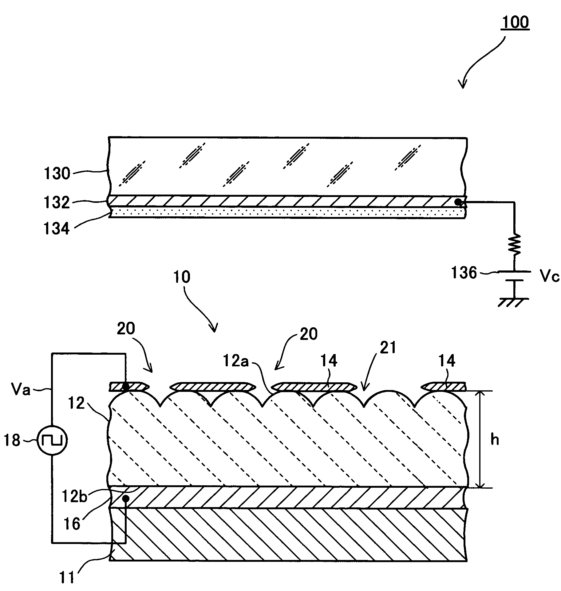
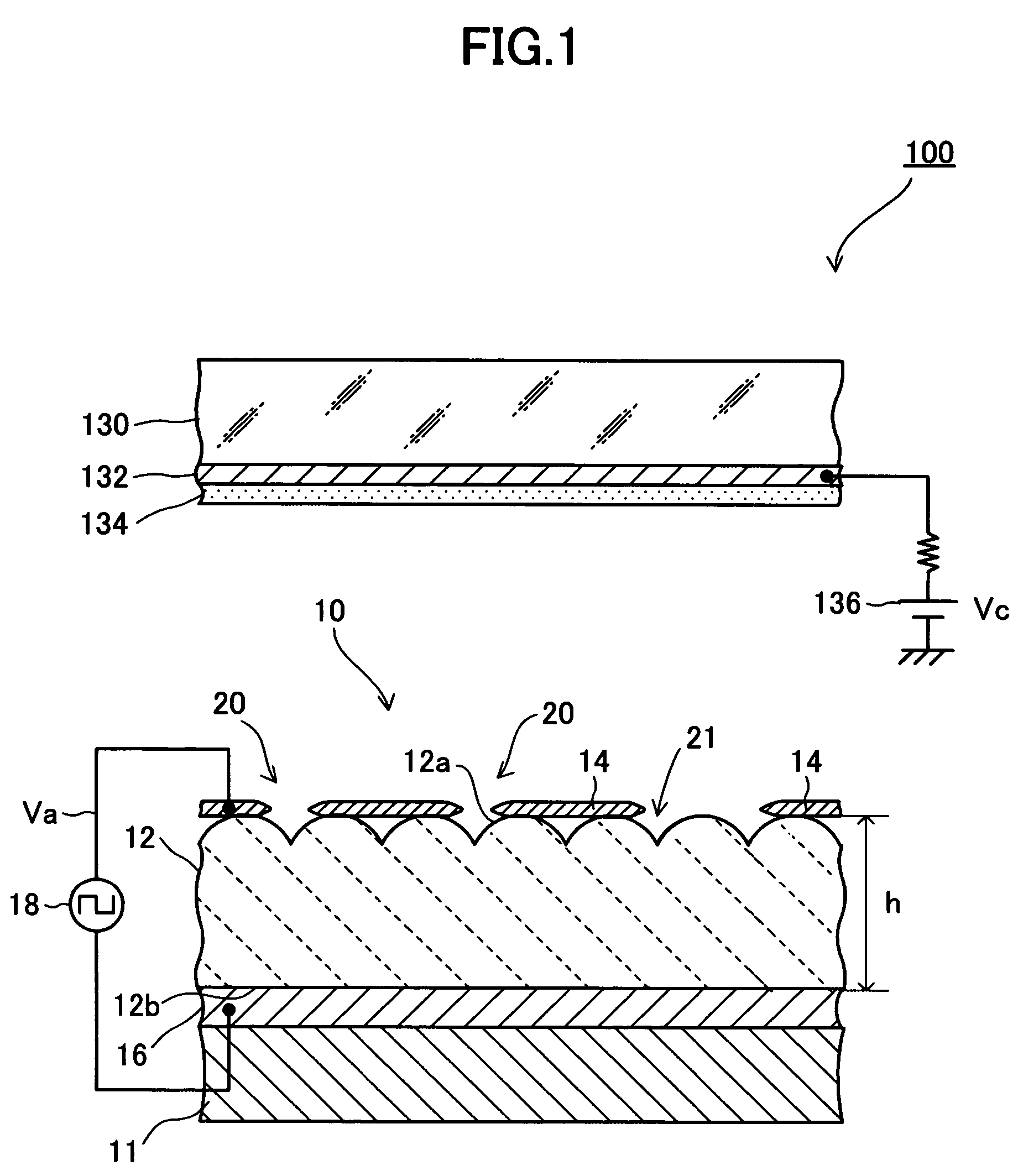
[0100]The first electrode 14 was formed by applying Pt / LSCO (Pt resinate containing 1 wt. % LSCO) onto the front surface 12a of the emitter section 12 through screen printing, followed by heating. The emitter section 12 was formed of a dielectric material containing 35.5PMN-39.5PT-25PZ as a primary component and containing MnO2 in an amount of 0.6 wt. %. The Qm of the dielectric material was 1,074.

example 2

[0103]In Example 2, the first electrode 14 was formed by mixing organometallic compounds such that the proportions by weight of Pt / Au / Ir was 93.0 / 4.5 / 2.5, and by subjecting the resultant mixture to screen printing and heating. In Example 2-1, the emitter section 12 was formed of a dielectric material having a Qm of 1,074, which is the same as the dielectric material employed in Example 1. In Example 2-2, the emitter section 12 was formed of a dielectric material containing, as a primary component, 37.5PMN-25PT-37.5PZ in which the amount of Pb substituted by Sr is 8 mol %, and containing MnO2 in an amount of 0.2 wt. %. The Qm of the dielectric material was 508.


PUM

PropertyMeasurementUnit
thicknessaaaaaaaaaa
thicknessaaaaaaaaaa
thicknessaaaaaaaaaa

Abstract

A dielectric-film-type electron emitter includes an emitter section, a first electrode, and a second electrode. The emitter section is formed of a thin layer of a polycrystalline dielectric material. The dielectric material constituting the emitter section is formed of a material having high mechanical quality factor (Qm). Specifically, the dielectric material has a Qm higher than that of a so-called low-Qm material (a material having a Qm of 100 or less). The Qm of the dielectric material is preferably 300 or more, more preferably 500 or more.

Description

BACKGROUND OF THE INVENTION[0001]1. Field of the Invention[0002]The present invention relates to an electron emitter which is configured such that it can emit electrons through application of a predetermined electric field.[0003]2. Description of the Related Art[0004]This type of an electron emitter is configured such that when a predetermined electric field is applied to an electron emission section (emitter section) in a vacuum having a predetermined vacuum level, electrons are emitted from the electron emission section (emitter section).[0005]Such an electron emitter is employed as an electron beam source in various apparatuses that utilize electron beams. Specific examples of such an apparatus include a display (in particular, a field emission display (FED)), an electron beam irradiation apparatus, a light source device, an electronic-component-manufacturing apparatus, and an electronic circuit component.[0006]In application to an FED, a plurality of electron emitters are two-di...

Claims


Application Information

Patent Timeline
Patent Type & Authority Patents(United States)
IPC IPC(8): H01J19/06H01J1/14
CPCB82Y10/00H01J1/32H01J1/312H01J2201/3125
Inventor YAMAGUCHI, HIROFUMISATO, KEI
Owner NGK INSULATORS LTD
Why Eureka
Try Eureka