Module

a technology of modules and components, applied in the field of modules, to achieve the effect of increasing the functionality of the module, increasing the mounting density of components, and reducing the thickness of the semiconductor substra

Active Publication Date: 2015-06-25
MURATA MFG CO LTD
View PDF4 Cites 24 Cited by
  • Summary
  • Abstract
  • Description
  • Claims
  • Application Information

AI Technical Summary

Benefits of technology

[0009]In the thus-configured invention, the functionality of the module is increased by increasing the component mounting density by mounting the components on both sides of the wiring substrate. On the other hand, the thickness of the first component layer provided on the one main surface of the wiring substrate and formed by mounting only the semiconductor substrate facedown as a component on the one main surface is made smaller than the thickness of the second component layer provided on the other main surface of the wiring substrate and formed by mounting the plurality of chip components on the other main surface.
[0010]That is, since the electrical characteristics of the semiconductor substrate do not greatly change even if a back-surface side of the semiconductor substrate, which is mounted face down on the one main surface of the wiring substrate, is subjected to polishing or grinding, the semiconductor substrate can be made thinner by subjecting the back-surface side of the semiconductor substrate to polishing or grinding without damaging the certain electrical circuits formed on the front-surface side. Consequently, the first component layer provided on the one main surface of the wiring substrate is formed by mounting facedown only the semiconductor substrate as a component and therefore the thickness of the first component layer can be made smaller than the thickness of the second component layer by subjecting the back-surface side of the semiconductor substrate of the first component layer to polishing or grinding in order reduce the thickness of the semiconductor substrate.
[0011]Therefore, in spite of the increase in the functionality achieved by mounting components on both of the main surfaces of the wiring substrate, a low-profile module can be provided which has high functionality as a result of increasing its component mounting density by making the thickness of the first component layer formed by mounting only the semiconductor substrate facedown on the one main surface of the wiring substrate smaller than the thickness of the second component layer formed by mounting the plurality of components on the other main surface of the wiring substrate.

Problems solved by technology

In addition, when the functionality of a module is increased by increasing the component mounting density, there is a risk that unwanted radiation from certain electrical circuits formed on a semiconductor substrate mounted in the module installed in the information communication terminal will affect other components mounted in the module or other modules installed in the information communication terminal and therefore appropriate measures against this have been demanded.

Method used


Image

  • Module
  • Module
  • Module

Examples


Embodiment Construction

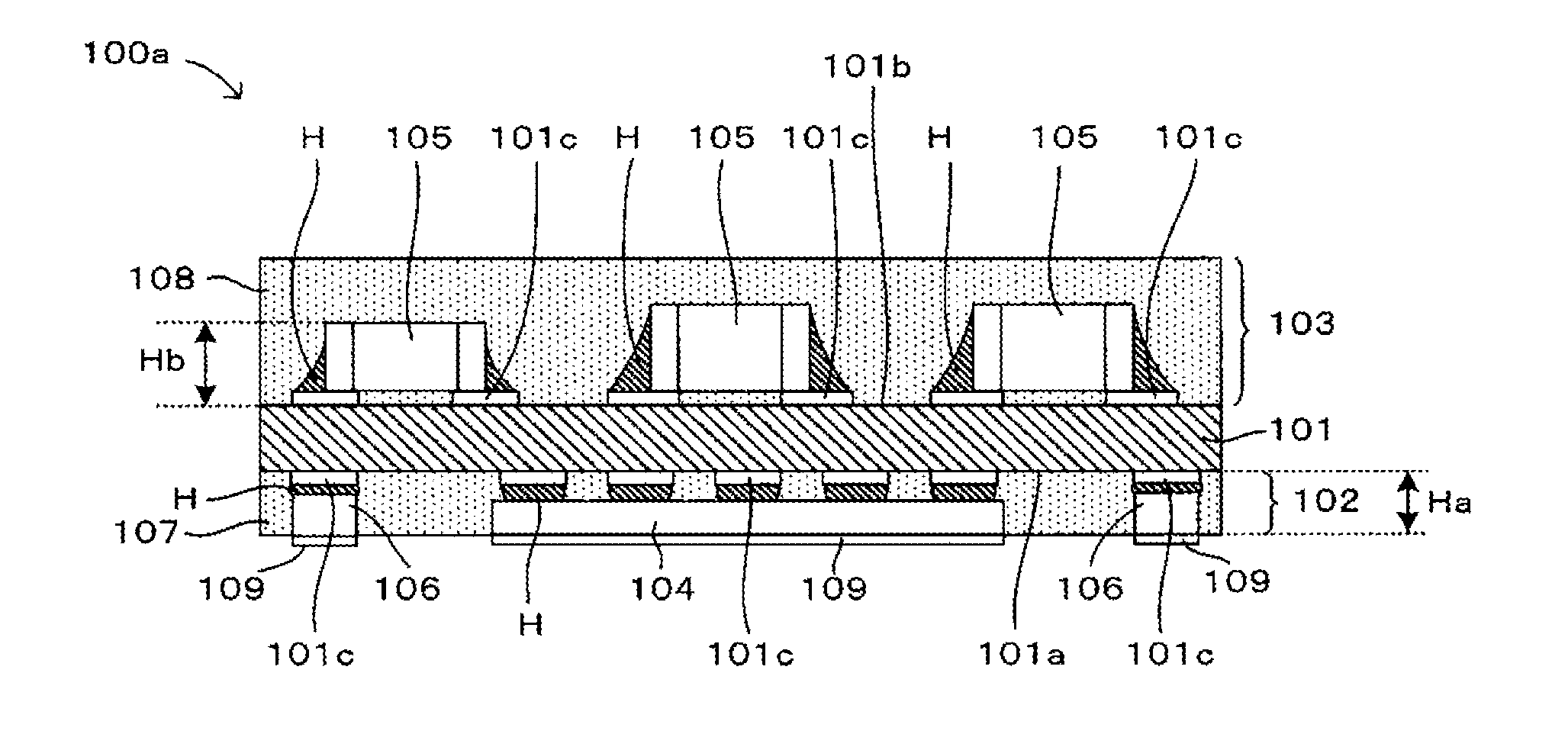
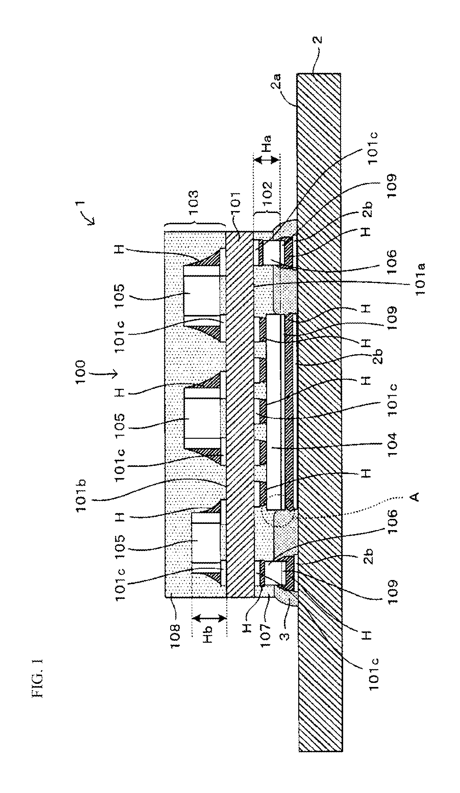
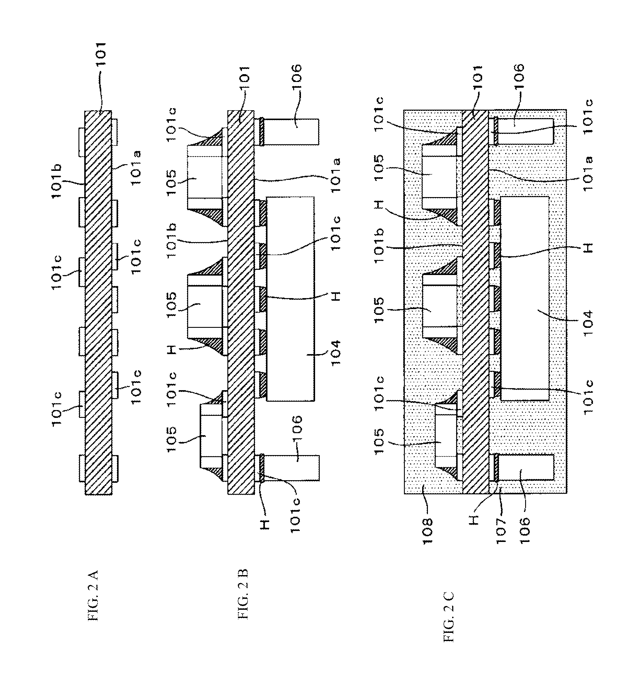
[0030]An embodiment of the present invention will be described with reference to FIGS. 1 to 3. FIG. 1 illustrates a module-installed apparatus that is equipped with a module according to the present invention and FIGS. 2A to 2E illustrate a method of manufacturing the module provided in the module-installed apparatus of FIG. 1 with different states. In addition, FIG. 3 is an enlarged view showing a main part of one example of a connection terminal.

[0031](Module-Installed Apparatus)

[0032]A module-installed apparatus 1, as illustrated in FIG. 1, is equipped with a mother substrate 2, a module 100 mounted on the mother substrate 2 and an underfill resin layer 3 that is formed of a resin in order to protect the connection portions between the mother substrate 2 and the module 100. The module-installed apparatus 1 is installed in an information communication terminal such as a cellular phone or a mobile information terminal.

[0033]Inside the mother substrate 2, there is provided a wiring ...


PUM


Abstract

A low profile module is provided that has a high functionality achieved by increasing the component mounting density. In spite of achieving high functionality in a module 100 by respectively mounting components such as a semiconductor substrate 104 and chip components 105 on the two main surfaces 101a and 101b of a wiring substrate 101, the low-profile module 100 can be provided which has a high functionality as a result of increasing its component mounting density by forming a thickness Ha of a first component layer 102 formed by mounting only the semiconductor substrate 104 face down on one main surface 101a of the wiring substrate 101 so as to be smaller than the thickness of a second component layer 103 formed by mounting a plurality of chip components 105 on the other main surface 101b of the wiring substrate 101.

Description

BACKGROUND OF THE INVENTION[0001]1. Field of the Invention[0002]The present invention relates to a module in which components are mounted on both of the main surfaces of a wiring substrate.[0003]2. Description of the Related Art[0004]In the related art, as examples of modules to be installed in an information communication terminal such as a cellular phone or a mobile information terminal, modules that are known include a module 500 of the related art illustrated in FIG. 6. In the module 500, columnar external connection terminals 502 (electrode posts) are provided in an upright manner on a wiring substrate 501, and a semiconductor substrate 503 is mounted face down on one main surface of the wiring substrate 501, is electrically connected to the connection terminals 502, and is covered with a resin layer 504. A module like the module 500 is for example formed in the following way. After mounting the semiconductor substrate 503 face down on one main surface of the wiring substrate 5...

Claims


Application Information

Patent Timeline
Patent Type & Authority Applications(United States)
IPC IPC(8): H01L25/16H01L23/498H01L23/00H01L25/065H01L23/31
CPCH01L25/165H01L25/0652H01L23/3135H01L2224/16227H01L23/49838H01L23/49811H01L2224/16113H01L24/17H01L23/3128H01L24/16H01L24/32H01L24/73H01L25/16H01L2224/73253H01L2924/15321H01L2924/18161H01L2924/19106H01L23/50H01L2924/12042H01L24/81H01L24/83H01L24/92H01L2224/0401H01L2224/04026H01L2224/056H01L2224/06181H01L2224/16238H01L2224/32227H01L2224/92225H01L2224/131H01L2224/291H01L2924/00H01L2924/00014H01L2924/014H01L2224/16225H01L2224/32225
Inventor MATSUMOTO, MITSUHIROTAKAGI, YOICHINOMURA, TADASHIKAMADA, AKIHIKOOGAWA, NOBUAKINISHIDA, KENSEI
Owner MURATA MFG CO LTD
Why Eureka
Try Eureka