Method for polishing photonic chips

a technology of photonic chips and polishing methods, which is applied in the field of photonic chips, can solve the problems of allowing the top edges of the photonic chips to be seen by an operator, rough edges that are not ideal for optical transmission, and rough edges that are not ideal for silicon wafers. to achieve the effect of stopping the polishing of the photonic chips

Inactive Publication Date: 2016-05-31
BAE SYST INFORMATION & ELECTRONICS SYST INTERGRATION INC
View PDF1 Cites 0 Cited by
  • Summary
  • Abstract
  • Description
  • Claims
  • Application Information

AI Technical Summary

Benefits of technology

[0009]In accordance with a preferred embodiment of the present invention, a gauge is placed in a photonic chip adjacent to an edge to be polished. The gauge includes a set of bars of various lengths. The bar lengths can be progressively ordered from shortest to longest or vice versa. The photonic chip is then secured in a chip polishing jig to get ready for polishing. When the photonic chip is being polished, an operator can visually inspect a the gauge by looking at the polishing edge to estimate a polishing depth in order to determine a stopping point for polishing. Once the stopping point has been reached, the polishing of the photonic chip can be stopped.

Problems solved by technology

However, cutting with a diamond tipped saw will leave silicon wafers with rough or jagged edges, and rough edges are not ideal for optical transmissions.
Conventional polishing methods suffer in that the polishing of many photonic chips at the same time requires the use of a chip polishing jig that holds the photonic chips perpendicular to a polish platen, and such arrangement does not permit the top edges of the photonic chips to be viewed by an operator.
Since the operator cannot see the top of a photonic chip, it is impossible for the operator to determine how deep into the photonic chip that the polish has removed without taking the photonic chip off from the chip polishing jig.
Needless to say, additional time is required for the operator to un-mount and remount the photonic chip, which leads to an increase in operational time and a decrease in operational efficiency.

Method used


Image

  • Method for polishing photonic chips
  • Method for polishing photonic chips
  • Method for polishing photonic chips

Examples


Embodiment Construction

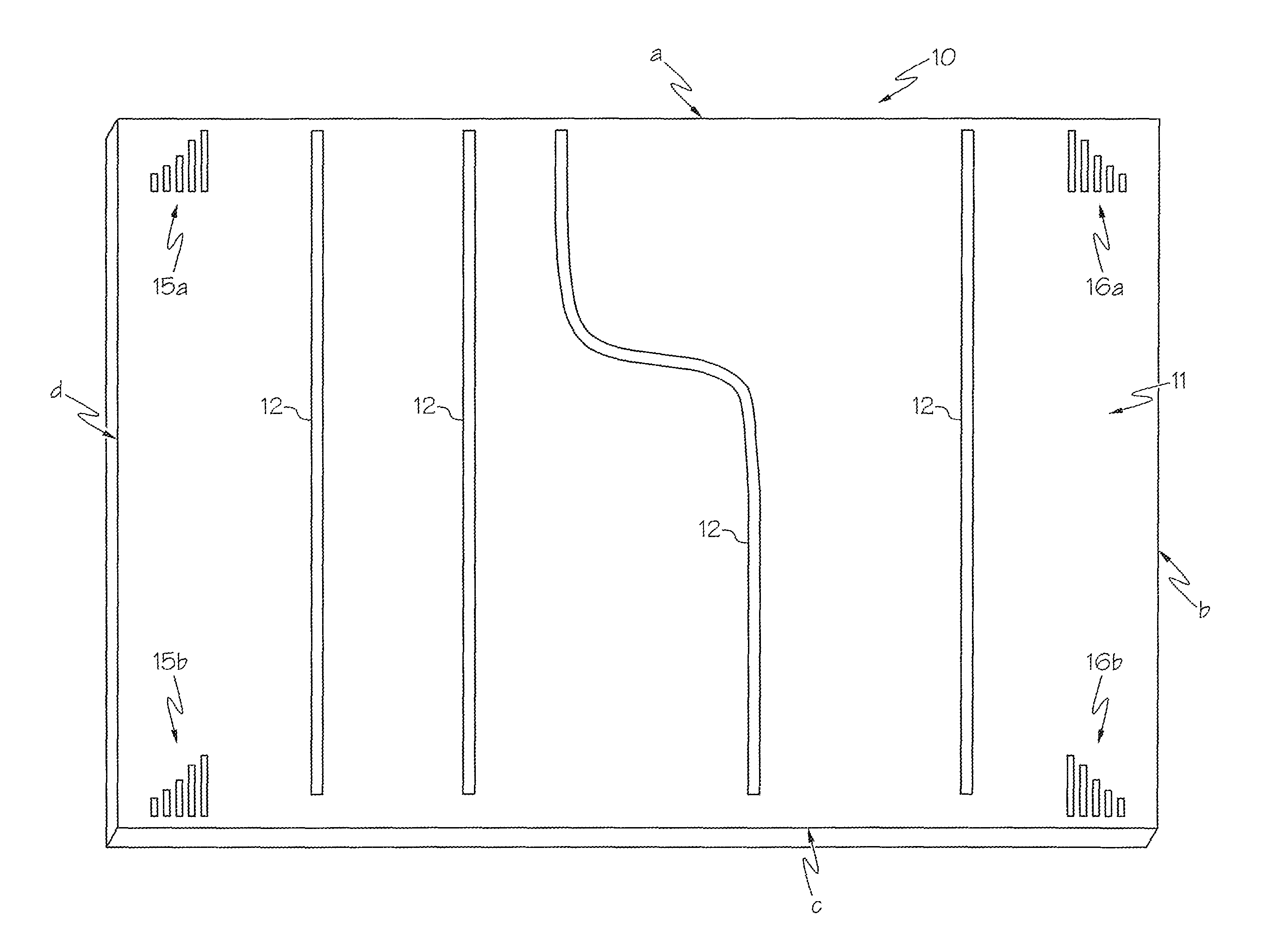
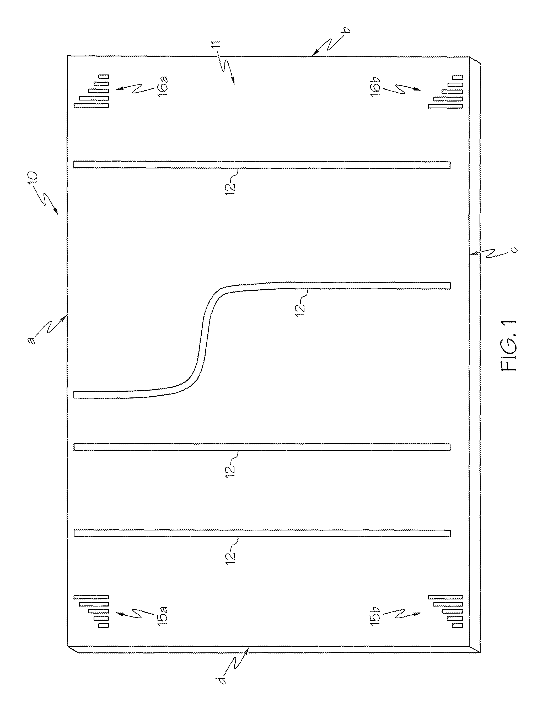
[0016]During edge polishing of a photonic chip, it is important not to polish too deeply into the photonic chip or the waveguides included within. Thus, as a preferred embodiment of the present invention, at least one gauge is placed within a photonic chip in order to assist an operator to determine the progress of an edge polishing process via visual inspection.

[0017]Referring now to the drawings and in particular to FIG. 1, there is illustrated an isometric view of a photonic chip in which a preferred embodiment of the present invention can be incorporated. As shown, a photonic chip 10 includes a top surface 11 and four edges (side surfaces) a-d. Photonic chip 10 can be of any size, and the length and width of top surface 11 preferably defines the size of photonic chip 10, while the depths of edges a-d are substantially smaller than the length or width of photonic chip 10. Multiple waveguides 12 are located within photonic chip 10 underneath top surface 11. Waveguides 12 may be ma...


PUM


Abstract

A method for polishing photonic chips is described. A gauge is placed in a photonic chip adjacent to an edge to be polished. The gauge includes a set of bars of various lengths. The bar lengths can be progressively ordered from shortest to longest or vice versa. The photonic chip is then secured in a chip polishing jig to get ready for polishing. When the photonic chip is being polished, an operator can visually inspect the gauge by looking at the polishing edge to estimate a polishing depth in order to determine a stopping point for polishing. Once the stopping point has been reached, the polishing of the photonic chip can be stopped.

Description

PRIORITY CLAIM[0001]The present application claims priority under 35 U.S.C. §119(e)(1) to provisional application No. 62 / 020,191, filed on Jul. 2, 2014, the contents of which are incorporated herein by reference.STATEMENT OF GOVERNMENT INTEREST[0002]This invention was made with United States Government support under Contract No. HR0011-05-C-0027 awarded by the DEFENSE ADVANCED RESEARCH DEPARTMENTS AGENCY. The United States Government has certain rights in this invention.BACKGROUND OF THE INVENTION[0003]1. Technical Field[0004]The present invention relates to photonic chips in general, and in particular to a method for polishing photonic chips.[0005]2. Description of Related Art[0006]Conventional photonic chips are typically made from silicon wafers. Silicon wafers tend to be comparatively large, but many photonic chips are required to be in relatively smaller sizes. In order to reach the desired size, the edges of silicon wafers must be cut typically with a diamond tipped saw. Howev...

Claims


Application Information

Patent Timeline
Patent Type & Authority Patents(United States)
IPC IPC(8): G02B6/10G02B6/13B24B49/02B24B9/06G02B6/122G02B6/12
CPCG02B6/13B24B9/065B24B49/02G02B6/122G02B2006/121G02B2006/12197G02B6/30G02B6/3608
Inventor POMERENE, ANDREW T SGREGORY, MATTHEW A.
Owner BAE SYST INFORMATION & ELECTRONICS SYST INTERGRATION INC
Why Eureka
Try Eureka