Chemical mechanical polishing of a metal layer with polishing rate monitoring

a technology of mechanical polishing and monitoring of the polishing rate, which is applied in the direction of lapping machines, instruments, manufacturing tools, etc., can solve the problems of reducing the throughput of the cmp apparatus, affecting the use of the substrate, and affecting the polishing rate, so as to achieve the effect of reducing overpolishing and underpolishing, preventing electrical shorting, and high accuracy

Inactive Publication Date: 2005-03-22
APPLIED MATERIALS INC
View PDF67 Cites 10 Cited by
  • Summary
  • Abstract
  • Description
  • Claims
  • Application Information

AI Technical Summary

Benefits of technology

Possible advantages of implementations of the invention can include one or more of the following. During bulk polishing of the metal layer, the pressure profile applied by the carrier head can be adjusted to compensate for non-uniform polishing rates and non-uniform thickness of the incoming substrate. In addition, the polishing monitoring system can sense the polishing endpoint of a metal layer in-situ. Furthermore, the polishing monitoring system can determine the point at which the polishing apparatus should switch polishing parameters. For example, the polishing monitoring system can be used to trigger a polishing rate slow-down during polishing of a metal layer prior to the polishing endpoint. Polishing can be stopped with high accuracy. Overpolishing and underpolishing can be reduced, as can dishing and erosion, thereby improving yield and throughput.

Problems solved by technology

One problem in CMP is determining whether the polishing process is complete, i.e., whether a substrate layer has been planarized to a desired flatness or thickness, or when a desired amount of material has been removed.
On the other hand, underpolishing (removing too little) of a conductive layer leads to electrical shorting.
This is a time-consuming procedure that reduces the throughput of the CMP apparatus.
Alternatively, the examination might reveal that an excessive amount of material has been removed, rendering the substrate unusable.
Another reoccurring problem in CMP is dishing of the substrate surface when polishing a filler layer to expose an underlying layer.
Dishing can render the substrate unsuitable for integrated circuit fabrication, thereby lowering process yield.

Method used


Image

  • Chemical mechanical polishing of a metal layer with polishing rate monitoring
  • Chemical mechanical polishing of a metal layer with polishing rate monitoring
  • Chemical mechanical polishing of a metal layer with polishing rate monitoring

Examples


Embodiment Construction

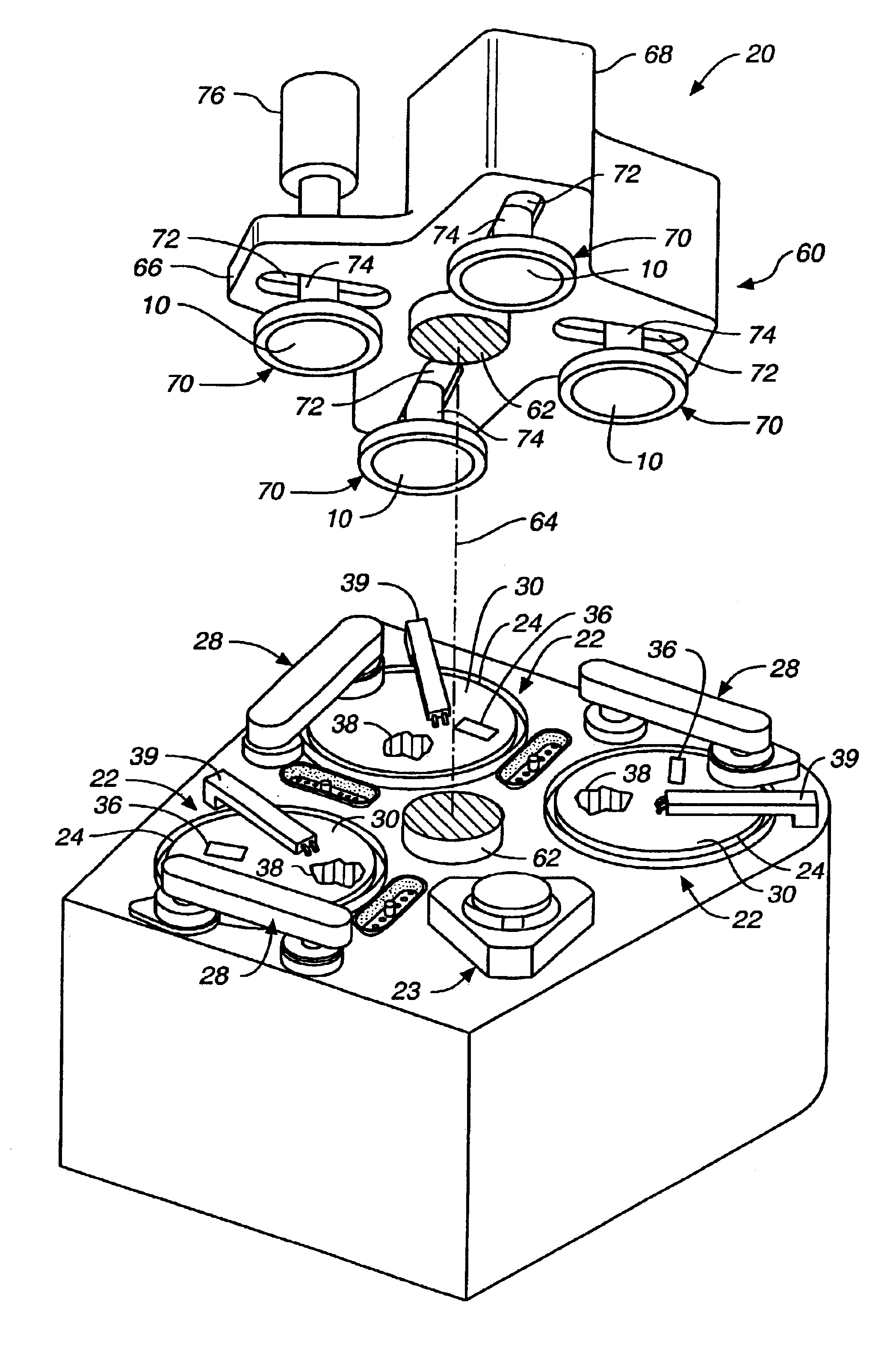
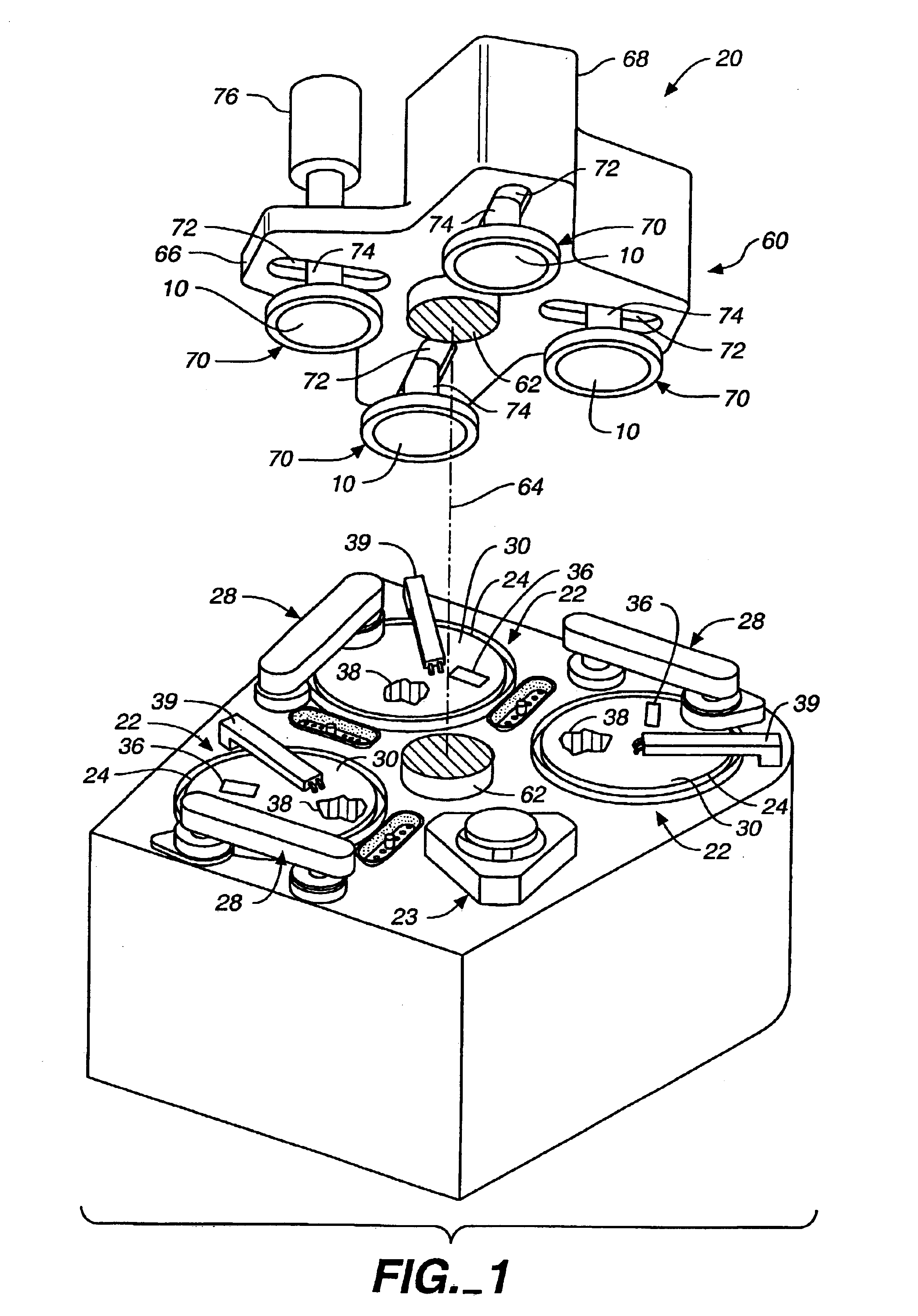
Referring to FIGS. 1, one or more substrates 10 can be polished by CMP apparatus 20. A description of a similar polishing apparatus 20 can be found in U.S. Pat. No. 5,738,574, the entire disclosure of which is incorporated herein by reference. Polishing apparatus 20 includes a series of polishing stations 22a, 22b and 22c, and a transfer station 23. Transfer station 23 transfers the substrates between the carrier heads and a loading apparatus.

Each polishing station includes a rotatable platen 24 on which is placed a polishing pad 30. The first and second stations 22a and 22b can include a two-layer polishing pad with a hard durable outer surface or a fixed-abrasive pad with embedded abrasive particles. The final polishing station 22c can include a relatively soft pad or a two-layer pad. Each polishing station can also include a pad conditioner apparatus 28 to maintain the condition of the polishing pad so that it will effectively polish substrates.

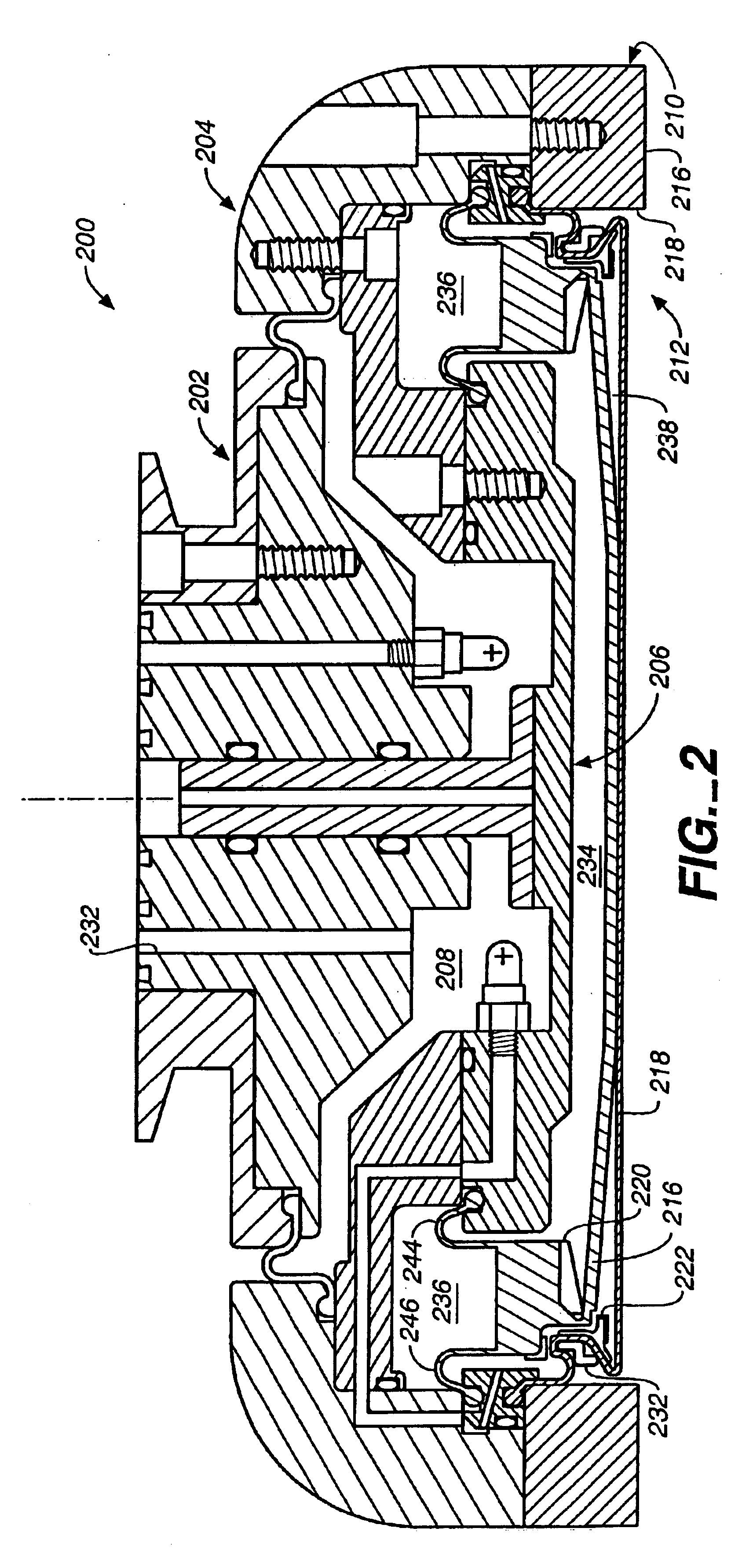
Referring to FIG. 3A, a two-layer p...


PUM

PropertyMeasurementUnit
capacitanceaaaaaaaaaa
resonant frequencyaaaaaaaaaa

Abstract

A method of chemical mechanical polishing a metal layer on a substrate in which the substrate is polished at a first polishing rate. Polishing is monitored with an eddy current monitoring system, and the polishing rate is reduced to a second polishing rate when the eddy current monitoring system indicates that a predetermined thickness of the metal layer remains on the substrate. Then polishing is monitored with an optical monitoring system, and polishing is halted when the optical monitoring system indicates that an underlying layer is at least partially exposed.

Description

BACKGROUNDThe present invention relates generally to chemical mechanical polishing of substrates, and more particularly to methods and apparatus for monitoring a metal layer during chemical mechanical polishing.An integrated circuit is typically formed on a substrate by the sequential deposition of conductive, semiconductive or insulative layers on a silicon wafer. One fabrication step involves depositing a filler layer over a non-planar surface, and planarizing the filler layer until the non-planar surface is exposed. For example, a conductive filler layer can be deposited on a patterned insulative layer to fill the trenches or holes in the insulative layer. The filler layer is then polished until the raised pattern of the insulative layer is exposed. After planarization, the portions of the conductive layer remaining between the raised pattern of the insulative layer form vias, plugs and lines that provide conductive paths between thin film circuits on the substrate. In addition, ...

Claims


Application Information

Patent Timeline
Patent Type & Authority Patents(United States)
IPC IPC(8): B24B37/04B24B49/02B24B49/12B24B37/013H01L21/00H01L21/321
CPCB24B37/013G01B7/105B24B49/12B24B49/02
Inventor REDEKER, FRED C.BAJAJ, RAJEEV
Owner APPLIED MATERIALS INC
Why Eureka
Try Eureka