Display device and method for manufacturing the same

a technology for display devices and manufacturing methods, applied in semiconductor devices, instruments, electrical devices, etc., can solve problems such as the difference in luminance between positions of display regions, the sudden decrease of current flowing thereto, etc., and achieve the effect of reducing or minimizing the difference in luminan

Active Publication Date: 2016-06-07
SAMSUNG DISPLAY CO LTD
View PDF10 Cites 0 Cited by
  • Summary
  • Abstract
  • Description
  • Claims
  • Application Information

AI Technical Summary

Benefits of technology

[0010]Accordingly, aspects of embodiments of the present invention have been made to provide a display device which can reduce or minimize a difference in luminance between positions of a display region on which an image is displayed.
[0011]Another aspect of embodiments of the present invention provides a method for manufacturing a display device which can reduce or minimize a difference in luminance between positions of a display region on which an image is displayed.
[0033]According to embodiments of the present invention, at least the following effects can be achieved.
[0034]For example, the difference in luminance between the positions of the display region on which the image is displayed can be reduced or minimized.

Problems solved by technology

However, the organic light emitting display adopting or utilizing a digital driving method may exhibit an IR-drop phenomenon, and if a voltage that is applied to a pixel is decreased, current that flows thereto may abruptly decrease.
The current decrease due to the IR-drop phenomenon may cause a difference in luminance between positions of a display region on which an image is displayed.

Method used


Image

  • Display device and method for manufacturing the same
  • Display device and method for manufacturing the same
  • Display device and method for manufacturing the same

Examples


Embodiment Construction

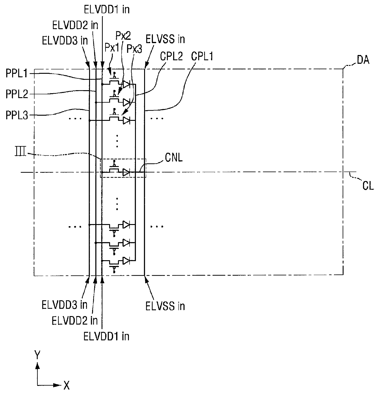
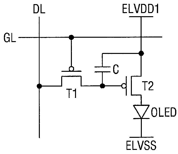
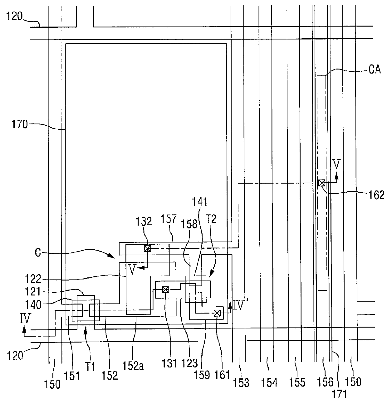
[0051]Aspects and features of the present invention and methods of accomplishing the same may be understood more readily by reference to the following detailed description of embodiments and the accompanying drawings. Embodiments of the present invention may, however, be embodied in many different forms and should not be construed as being limited to the embodiments set forth herein. Rather, these embodiments are provided so that this disclosure will be thorough and complete and will fully convey the concept of the invention to those skilled in the art, and the present invention will only be defined by the appended claims. Thus, in some embodiments, well-known structures and devices are not shown in order not to obscure the description of the invention with unnecessary detail. Like numbers refer to like elements throughout. In the drawings, the thickness of layers and regions are exaggerated for clarity.

[0052]It will be understood that when an element or layer is referred to as bein...


PUM


Abstract

A display device including a substrate having a display region on which an image is configured to be displayed, a plurality of pixels on the display region of the substrate, and a plurality of common power lines on the display region of the substrate and configured to supply a common power voltage to the plurality of pixels, the plurality of common power lines including first and second common power lines extending in a first direction, the second common power line being connected to the plurality of pixels arranged along the first direction, and the first and second common power lines being connected to each other in a central portion of the display region.

Description

CROSS-REFERENCE TO RELATED APPLICATIONS[0001]This application claims priority to and the benefit of Korean Patent Application No. 10-2014-0026100, filed on Mar. 5, 2014 in the Korean Intellectual Property Office, the disclosure of which is incorporated herein in its entirety by reference.BACKGROUND[0002]1. Field[0003]The present invention relates to a display device.[0004]2. Description of the Prior Art[0005]A display device is a device that visually displays data. The display device may be a liquid crystal display, an electrophoretic display, an organic light emitting display, an inorganic EL (Electro Luminescent) display, a field emission display, a surface-conduction electron-emitter display, a plasma display, or a cathode ray display.[0006]Among them, the organic light emitting display is a display device that displays information, such as an image or text, using light that is generated through combination of holes and electrons, which are respectively provided from an anode ele...

Claims


Application Information

Patent Timeline
Patent Type & Authority Patents(United States)
IPC IPC(8): G09G3/30G09G3/32H01L27/32
CPCG09G3/3258G09G3/3225H01L27/3276G09G2300/0404G09G2300/0426G09G2300/0452G09G2300/08G09G2320/0233H10K59/131
Inventor KIM, DONG GYU
Owner SAMSUNG DISPLAY CO LTD
Why Eureka
Try Eureka