
Semiconductor device, liquid discharge head, and liquid discharge apparatus

a liquid discharge head and semiconductor technology, applied in the field of semiconductor devices, can solve problems such as lowering printing speed, layout or a size of detection switches, and heat generated when charging or discharging piezo elements, so as to ensure resistance to static electricity applied, and suppress an increase in area

Active Publication Date: 2016-07-19
SEIKO EPSON CORP
View PDF10 Cites 1 Cited by
  • Summary
  • Abstract
  • Description
  • Claims
  • Application Information

AI Technical Summary

Benefits of technology

[0010]An advantage of some aspects of the present invention is to suppress an increase in area and ensure resistance to static electricity applied by enabling an layout efficient in providing a switch performing residual vibration detection and the printing switch in the same semiconductor device.

Problems solved by technology

Meanwhile, it takes time to charge or discharge a piezo element when resistance of a printing transistor configuring the printing switch increases, thereby lowering a printing speed.
In addition, when the resistance of the printing transistor increases, heat generated when charging or discharging the piezo element becomes a problem.
Since the size of the printing transistor is large, when providing the detection switch and the printing switch in the same semiconductor device, a layout or a size of the detection switch becomes a problem.
However, when the size of the detection transistor is reduced, it is of concern that the detection transistor is destroyed by an application of static electricity.

Method used


Image

  • Semiconductor device, liquid discharge head, and liquid discharge apparatus
  • Semiconductor device, liquid discharge head, and liquid discharge apparatus
  • Semiconductor device, liquid discharge head, and liquid discharge apparatus

Examples


first embodiment

Improved Example of First Embodiment

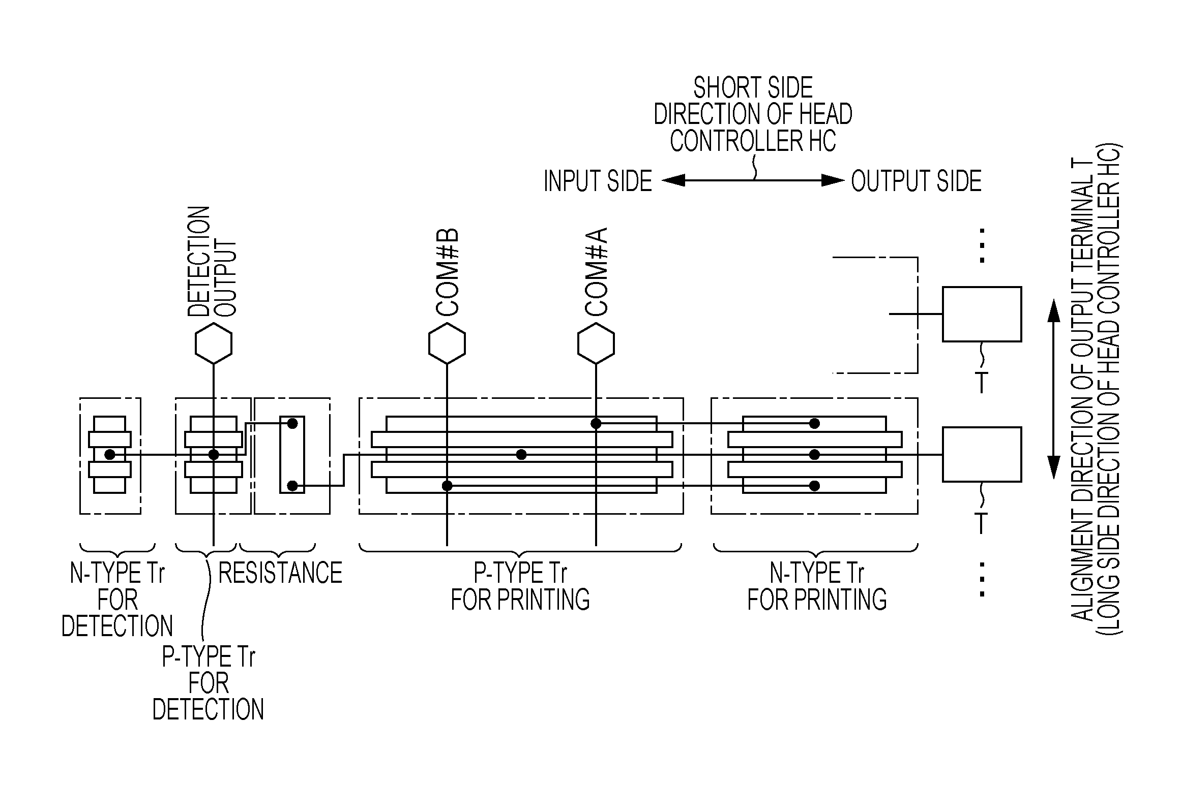
[0128]FIG. 12 is a layout diagram of an improved example of the first embodiment.

[0129]In an improved example, both the P-type printing transistor and the N-type printing transistor are disposed between the P-type detection transistor and the N-type detection transistor and the output terminal T. In other words, the P-type detection transistor and the N-type detection transistor are spaced further away from the output terminal T than either of the P-type printing transistor and the N-type printing transistor and are disposed at a rear side (an input side of the head controller HC). Specifically, the N-type printing transistor, the P-type printing transistor, the P-type detection transistor, and the N-type detection transistor are disposed in order from a side of the output terminal T. In an improved example, the N-type detection transistor is disposed to be spaced further away from the output terminal T than in a layout of the first embodiment (FI...

second embodiment

Improved Example of Second Embodiment

[0137]FIG. 14 is a layout diagram of an improved example of the second embodiment.

[0138]In an improved example of the second embodiment, in the same manner as that of the improved example of the first embodiment, both a P-type printing transistor and an N-type printing transistor are disposed between a P-type detection transistor and an N-type detection transistor and the output terminal T. In other words, the P-type detection transistor and the N-type detection transistor are spaced further away from the output terminal T than either one of the P-type printing transistor and the N-type printing transistor and are disposed at the rear side (the input side of the head controller HC). Specifically, the N-type printing transistor, the P-type printing transistor, a resistor, the P-type detection transistor, and the N-type detection transistor are disposed in order from a side of the output terminal T. In an improved example, the N-type detection tran...


PUM


Abstract

A semiconductor device which is provided to correspond to each of a plurality of nozzles discharging a liquid and controls a plurality of drive elements causing a liquid to be discharged from each nozzle by an application of a drive signal includes a detection circuit which detects a residual vibration signal of the drive element, an output terminal which is provided to correspond to each of the plurality of drive elements, a discharge transistor which controls an application of the drive signal to the drive element through the output terminal, and a detection transistor which controls an application of the residual vibration signal to the detection circuit through the output terminal, in which the detection transistor is smaller than the discharge transistor in size, and the discharge transistor is disposed between the detection transistor and the output terminal.

Description

[0001]The entire disclosure of Japanese Patent Application No. 2014-042467, filed Mar. 5, 2014 is expressly incorporated by reference herein.BACKGROUND[0002]1. Technical Field[0003]The present invention relates to a semiconductor device, a liquid discharge head, and a liquid discharge apparatus.[0004]2. Related Art[0005]As a semiconductor device, a device which is provided for controlling a head of a liquid discharge apparatus (for example, a printer) is known. Drive elements (for example, piezo elements) are provided for each nozzle in a head of a printer. A semiconductor device for controlling a head controls an application of a drive signal to each of the piezo elements. More specifically, a drive signal is applied to the piezo element after selecting a pulse of the drive signal with a printing switch provided in the semiconductor device.[0006]In addition, a device which detects a state (such as defective nozzle) of a nozzle by detecting a residual vibration signal after the appl...

Claims


Application Information

Patent Timeline
Patent Type & Authority Patents(United States)
IPC IPC(8): B41J2/045B41J2/14
CPCB41J2/04541B41J2/0451B41J2/04511B41J2/04581B41J2/04595B41J2/14233B41J2002/14241B41J2002/14354B41J2002/14491B41J2/04596
Inventor TAKAGI, TOSHIHITO
Owner SEIKO EPSON CORP
Learn More