Semiconductor device reducing leakage current of transistor

a technology of semiconductor devices and leakage currents, applied in the direction of power consumption reduction, pulse techniques, instruments, etc., can solve the problems of disadvantageous increase in area of semiconductor devices, disadvantageous increase in power consumption due to leakage current etc., to reduce the leakage current of transistors in the operating sta

Active Publication Date: 2010-07-01
RENESAS ELECTRONICS CORP
View PDF15 Cites 0 Cited by
  • Summary
  • Abstract
  • Description
  • Claims
  • Application Information

AI Technical Summary

Benefits of technology

[0010]One object of the present invention is to provide a semiconductor device capable of reducing a leakage current of a transistor in an operating state.
[0011]Another object of the present invention is to provide a semiconductor device capable of suppressing increase in area due to wiring in a configuration for reducing a leakage current of a transistor.
[0013]According to the aspect of the present invention, the power supply voltage is controlled whether or not to be supplied to the second transistor or the back gate potential at the second transistor is changed in accordance with an operating speed of the semiconductor device, so that a driving capability of the semiconductor device can be changed.
[0014]Thus, it is possible to reduce a leakage current of a transistor in an operating state.

Problems solved by technology

However, the configuration disclosed in each of Japanese Patent Laying-Open Nos. 11-284493 and 2002-110920 is merely one example of the MTCMOS circuit and, therefore, is not intended to reduce a leakage current in an operating state.
Consequently, there arises a problem that if the flip-flop circuit is operated at a low speed, a rate of power consumption due to a leakage current with respect to power consumption in the operating state disadvantageously increases.
Consequently, there arises a problem that a semiconductor device disadvantageously increases in area.

Method used


Image

  • Semiconductor device reducing leakage current of transistor
  • Semiconductor device reducing leakage current of transistor
  • Semiconductor device reducing leakage current of transistor

Examples


first embodiment

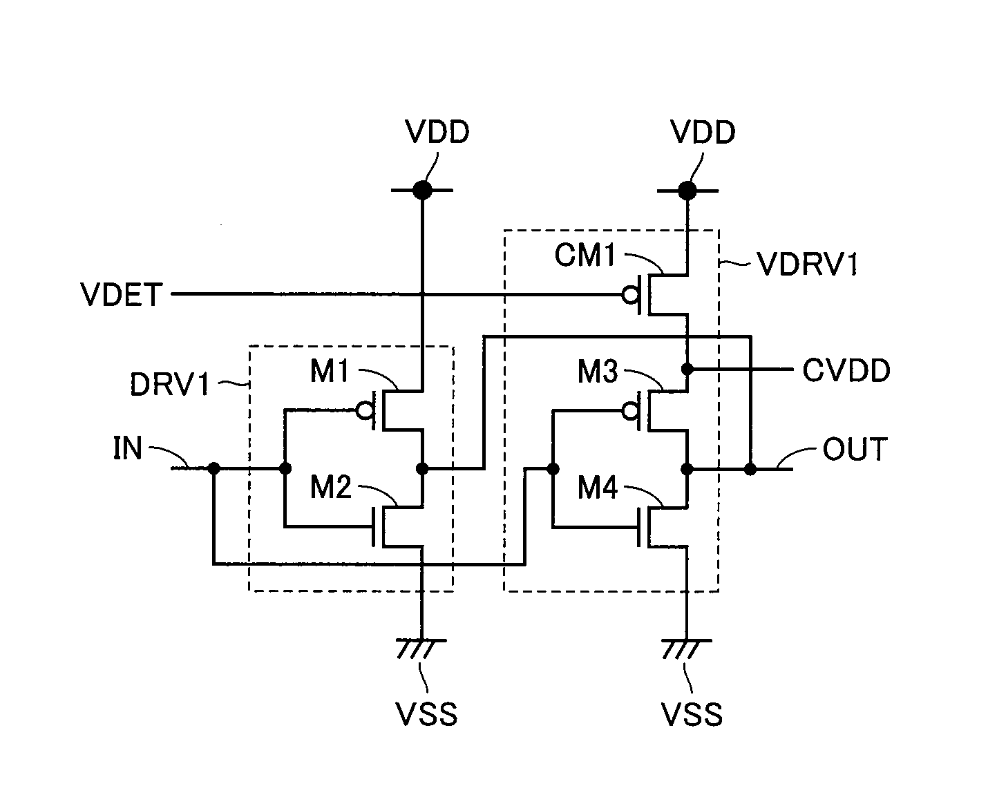
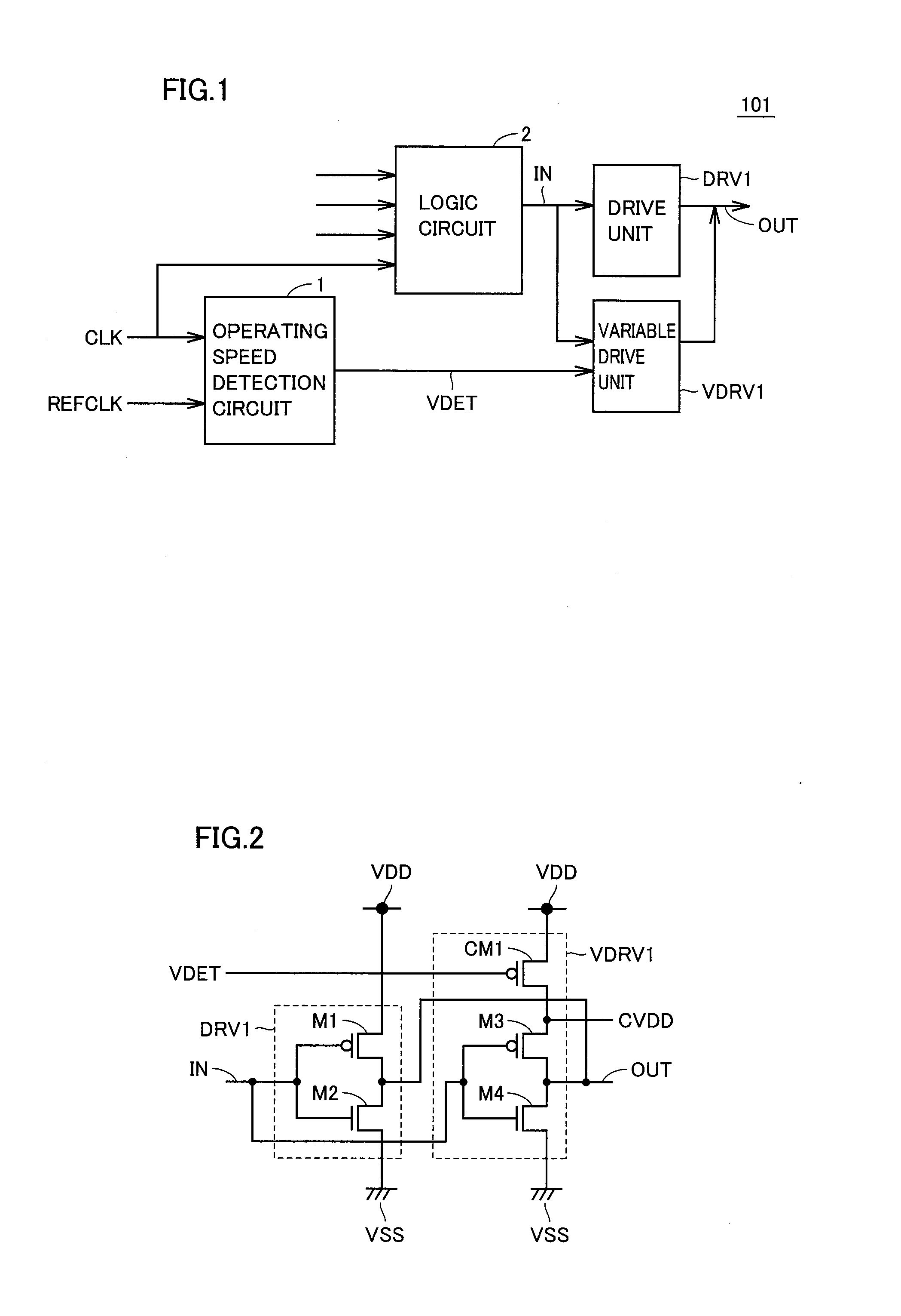
[0028]FIG. 1 shows a block diagram of a configuration of a semiconductor device according to a first embodiment of the present invention.

[0029]With reference to FIG. 1, semiconductor device 101 includes an operating speed detection circuit 1, a logic circuit 2, a drive unit DRV1 and a variable drive unit VDRV1.

[0030]Logic circuit 2 receives an external operating clock CLK, executes signal processing, based on operating clock CLK, and outputs a signal synchronized with operating clock CLK to each of drive unit DRV1 and variable drive unit VDRV1 via an input node IN.

[0031]Each of drive unit DRV1 and variable drive unit VDRV1 is a CMOS inverter, for example. That is, each of drive unit DRV1 and variable drive unit VDRV1 receives a signal from logic circuit 2 via input node IN, inverts a logic level of the received signal, and outputs the inverted signal to an output node OUT.

[0032]Operating speed detection circuit 1 detects a frequency of operating clock CLK. More specifically, operati...

second embodiment

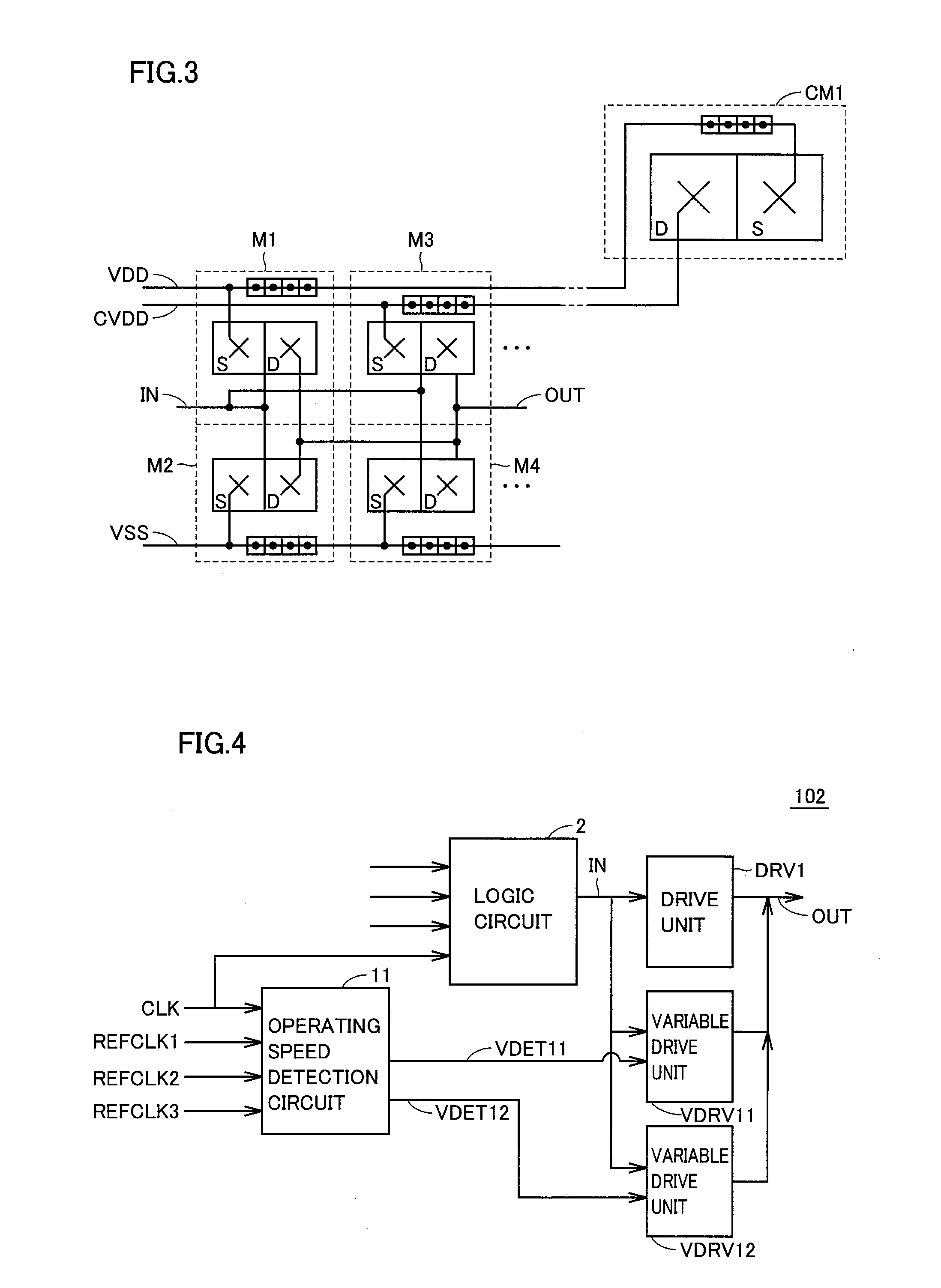
[0064]A second embodiment relates to a semiconductor device in which variable drive units are increased in number, as compared with the semiconductor device according to the first embodiment. Details of the semiconductor device according to the second embodiment except details to be described later are similar to those of the semiconductor device according to the first embodiment.

[0065]FIG. 4 shows a configuration of the semiconductor device according to the second embodiment of the present invention.

[0066]With reference to FIG. 4, semiconductor device 102 includes an operating speed detection circuit 11, a logic circuit 2, a drive unit DRV1, a variable drive unit VDRV11 and a variable drive unit VDRV12.

[0067]Each of drive unit DRV1, variable drive unit VDRV11 and variable drive unit VDRV12 is a CMOS inverter, for example. That is, each of drive unit DRV1, variable drive unit VDRV11 and variable drive unit VDRV12 receives a signal from logic circuit 2 via an input node IN, inverts a...

third embodiment

[0091]A third embodiment relates to a semiconductor device in which a configuration for changing a driving capability is changed, as compared with the semiconductor device according to the first embodiment. Details of the semiconductor device according to the third embodiment except details to be described later are similar to those of the semiconductor device according to the first embodiment.

[0092]FIG. 6 shows a configuration of the semiconductor device according to the third embodiment of the present invention.

[0093]With reference to FIG. 6, semiconductor device 103 includes an operating speed detection circuit 1, a back gate voltage control circuit 3, a logic circuit 2, a drive unit DRV21 and a variable drive unit VDRV21. Drive unit DRV21 includes a P-channel MOS transistor M11 and an N-channel MOS transistor M12. Variable drive unit VDRV21 includes a P-channel MOS transistor M13 and an N-channel MOS transistor M14.

[0094]Each of drive unit DRV21 and variable drive unit VDRV21 is...


PUM


Abstract

A semiconductor device includes: a first transistor having a control electrode coupled to an input node receiving a signal synchronized with a clock, a first conductive electrode coupled to an output node, and a second conductive electrode; a second transistor having a control electrode coupled to the input node, a first conductive electrode coupled to the output node, and a second conductive electrode coupled to a power supply node; and a first switch element connected between the power supply node and the second conductive electrode of the second transistor and turned on and off based on a first control signal indicating a detection result of a frequency of the clock.

Description

BACKGROUND OF THE INVENTION[0001]1. Field of the Invention[0002]The present invention relates to a semiconductor device, in particular, a semiconductor device that reduces a leakage current of a transistor.[0003]2. Description of the Background Art[0004]Examples of a technique of reducing a leakage current of a transistor may include an MTCMOS (Multi Threshold Voltage Complementary Metal Oxide Semiconductor) circuit that reduces a leakage current in a standby state, and a VTCMOS (Variable Threshold Voltage Complementary Metal Oxide Semiconductor) circuit that reduces a leakage current in an operating state.[0005]As one example of the MTCMOS circuit, for example, Japanese Patent Laying-Open No. 11-284493 discloses the following configuration. That is, in a master-slave flip-flop including a master flip-flop and a slave flip-flop, the master flip-flop is an inverter constituted of a transistor having a low threshold value and connected to a power supply which can be interrupted. Thus,...

Claims


Application Information

Patent Timeline
Patent Type & Authority Applications(United States)
IPC IPC(8): H01L25/00
CPCH03K19/0013H03K19/018585
Inventor ITO, TERUYUKI
Owner RENESAS ELECTRONICS CORP
Why Eureka
Try Eureka