Bus system for semiconductor circuit

a bus system and semiconductor technology, applied in the field of bus systems for semiconductor circuits, can solve the problems of increasing the complexity of traffic flow running through the bus, increasing the difficulty of designing an integrated circuit by such a lumped bus control, etc., and achieve the effect of maintaining bus transmission performance and increasing data transmission efficiency

Active Publication Date: 2016-09-06
PANASONIC INTELLECTUAL PROPERTY MANAGEMENT CO LTD
View PDF18 Cites 2 Cited by
  • Summary
  • Abstract
  • Description
  • Claims
  • Application Information

AI Technical Summary

Benefits of technology

[0014]A non-limiting exemplary embodiment of the present application provides a technique for transmitting packets efficiently through an NoC in which multiple nodes on an integrated circuit are connected together with buses and in which a distributed bus control is carried out.
[0017]Even if multiple buses with mutually different transfer rates are connected together when data is going to be transmitted through a semiconductor system, a bus system for a semiconductor circuit according to an aspect of the present invention can still reduce congestion on the buses and can broaden the operating band of the buses with the buses' operating frequencies kept relatively low.

Problems solved by technology

However, as the functionality of an integrated circuit has been further improved and as the number of cores in an integrated circuit has been further increased these days, the scale of the circuit has become even larger and the traffic flows running through the bus has gotten even more complicated.
As a result, it has become increasingly difficult to design an integrated circuit by such a lumped bus control.
That is why since transmission and congestion control are supposed to be carried out continuously according to the conventional technologies until the transmission lines are too congested to avoid a breakdown, it is difficult to transmit data while maintaining expected transmission quality (see Japanese Laid-Open Patent Publication No. 2009-49742 and Evaluation of Fast Reliable Transport Protocol on Multiple Paths, IEICE Technical Report, February, 2005).
It is difficult to speed up the transmission by using a number of transmission lines in parallel by the conventional technologies in order to maintain sufficient transmission performance for the bus.

Method used


Image

  • Bus system for semiconductor circuit
  • Bus system for semiconductor circuit
  • Bus system for semiconductor circuit

Examples


Embodiment Construction

[0046]The present inventors studied the problems with the conventional technologies described above.

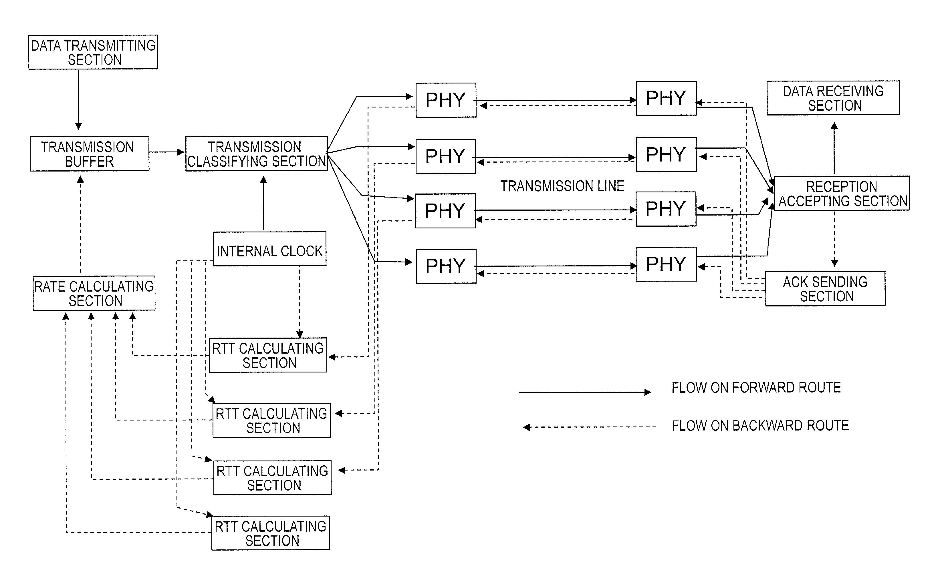
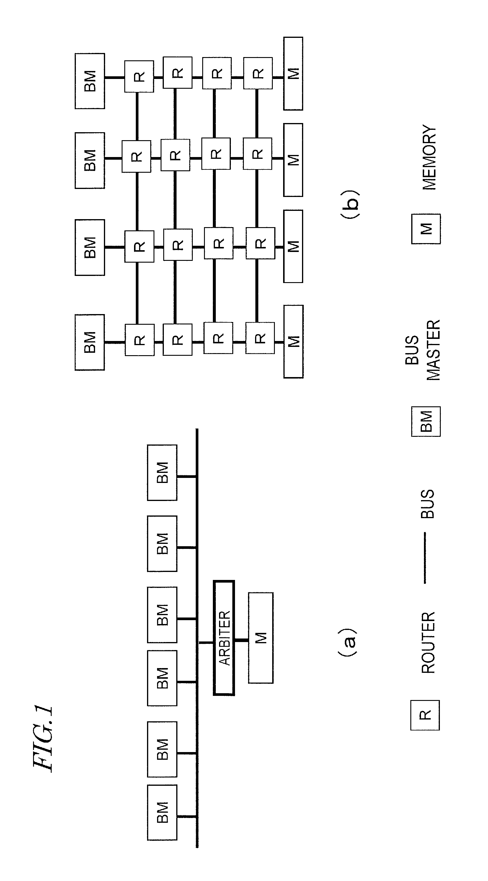
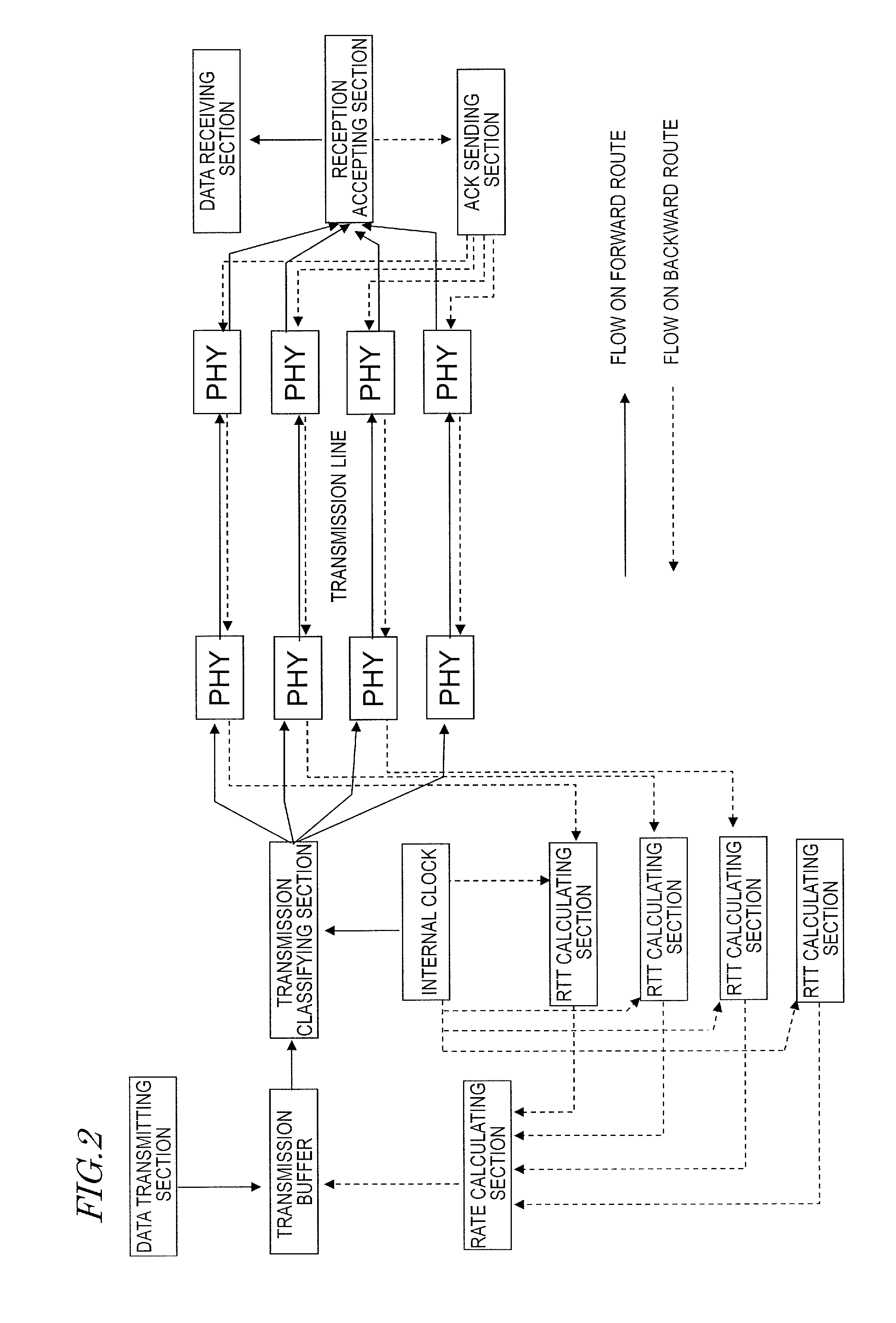
[0047]To maintain the transmission performance of an NoC bus in which a plurality of nodes on an integrated circuit are connected together with buses to carry out a distributed bus control, as the traffic flow increases, either the buses' operating frequency or their width needs to be increased. However, if the buses' operating frequency is raised, the power dissipation will increase. On the other hand, if the buses' width is broadened, then the lines will get congested easily.

[0048]As an approach to overcoming these problems, a configuration for changing the bus' width or operating frequency according to the type of the given functional block (which may be a video block, an audio block or a peripheral block, for example) has been adopted. For example, a semiconductor bus system including local buses, each of which is comprised of functional block units, and a system bus which connect...


PUM


Abstract

An exemplary semiconductor circuit bus system includes: a first bus comprised of distributed buses and having a first transfer rate; a second bus with a second transfer rate higher than the first transfer rate; a transmission node; a bus interface (IF) to connect the transmission node to the first bus; a router which connects the first and second buses; and a reception node connected to the second bus. The bus IF controls the flow rate of data flowing through the transmission routes of the first bus by reference to information about the amounts of transmissible data of the transmission routes. The router allocates the amounts of transmissible data to the transmission routes of the first bus and provides information about the amounts of transmissible data of the transmission routes for the bus IF and also controls the flow rate of the data flowing through the second bus.

Description

[0001]This is a continuation of International Application No. PCT / JP2013 / 006457, with an international filing date of Oct. 31, 2013, which claims priority of Japanese Patent Application No. 2012-246474, filed on Nov. 8, 2012, the contents of which are hereby incorporated by reference.BACKGROUND[0002]1. Technical Field[0003]The present disclosure relates to a bus system for a semiconductor circuit.[0004]2. Description of the Related Art[0005]Portion (a) of FIG. 1 illustrates an example of a lumped bus control. In a conventional integrated circuit which performs such a lumped bus control, a number of bus masters and a memory are connected together with a single bus, and accesses to the memory by the respective bus masters are arbitrated by an arbiter. However, as the functionality of an integrated circuit has been further improved and as the number of cores in an integrated circuit has been further increased these days, the scale of the circuit has become even larger and the traffic f...

Claims


Application Information

Patent Timeline
Patent Type & Authority Patents(United States)
IPC IPC(8): G06F13/40H04L12/40H04L12/403H04L12/801
CPCG06F13/4027H04L12/403H04L12/4013H04L47/13Y02B60/31Y02D30/50
Inventor YAMAGUCHI, TAKAOYOSHIDA, ATSUSHIISHII, TOMOKITOKUTSU, SATORU
Owner PANASONIC INTELLECTUAL PROPERTY MANAGEMENT CO LTD
Why Eureka
Try Eureka