Method for regulating reading voltage of NAND flash memory device

a technology read voltage, which is applied in the direction of static storage, digital storage, instruments, etc., can solve the problems of low read/write/write performance of mlc nand flash memory devices compared with slc and read errors, so as to improve the read performance of nand flash memory devices

Active Publication Date: 2017-01-31
THE AIO
View PDF13 Cites 12 Cited by
  • Summary
  • Abstract
  • Description
  • Claims
  • Application Information

AI Technical Summary

Benefits of technology

[0019]Therefore, a method of adjusting read voltages for a NAND flash memory device according to example embodiments simultaneously counts the number of memory cells corresponding to a first threshold voltage state and a fourth threshold voltage state by one read operation for a most significant bit (MSB) page and simultaneously changes first and third read voltages. Accordingly, the method of adjusting read voltages for the NAND flash memory device can improve the read performance of the NAND flash memory device.

Problems solved by technology

On the other hand, the MLC NAND flash memory device has a relatively low read / write / erase performance in comparison with the SLC NAND flash memory device because each memory cell of the MLC NAND flash memory device stores multi-bit data.
For example, because a threshold voltage distribution is gradually broadened due to charge loss and charge acquisition, the read error occurs by a variation of the threshold voltage distribution in the MLC NAND flash memory device.

Method used


Image

  • Method for regulating reading voltage of NAND flash memory device
  • Method for regulating reading voltage of NAND flash memory device
  • Method for regulating reading voltage of NAND flash memory device

Examples


Embodiment Construction

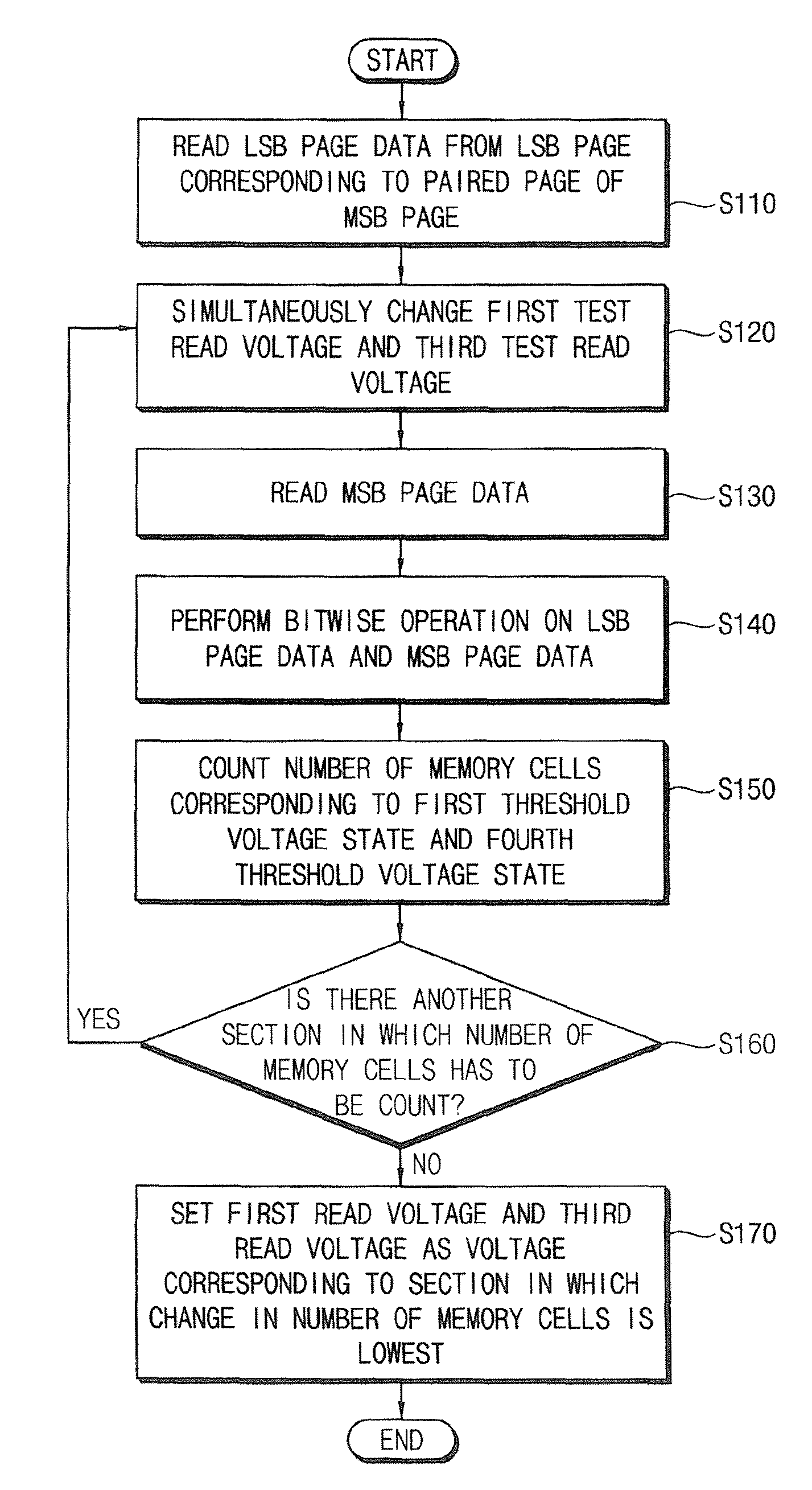
[0030]Hereinafter, embodiments of the present inventive concept will be explained in detail with reference to the accompanying drawings. For convenience of description, it is assumed that a NAND flash memory device is a MLC NAND flash memory device, and LSB and MSB page data are programmed to “11”, “10”, “00”, and “01” in increasing order of a threshold voltage of the memory cell.

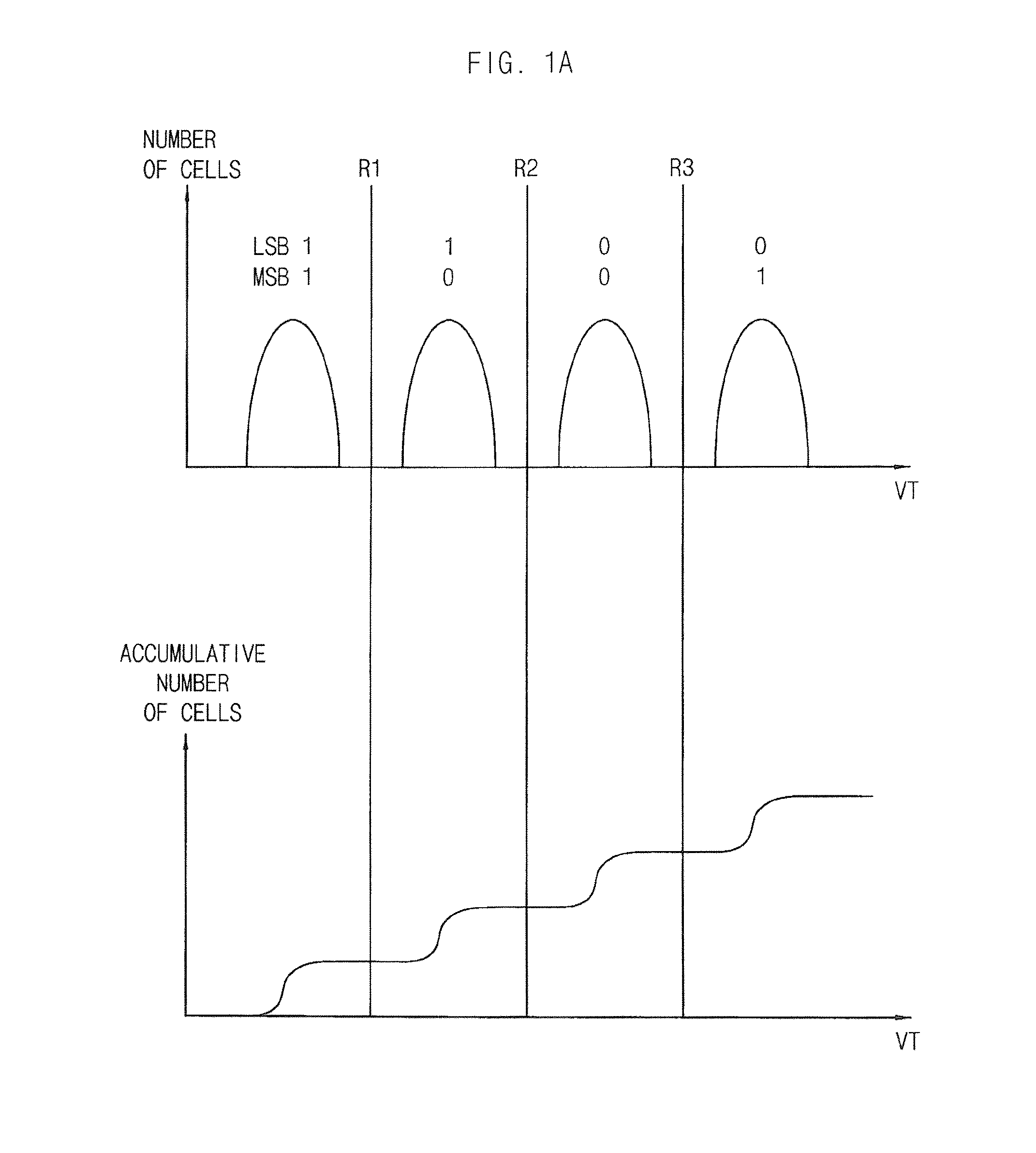
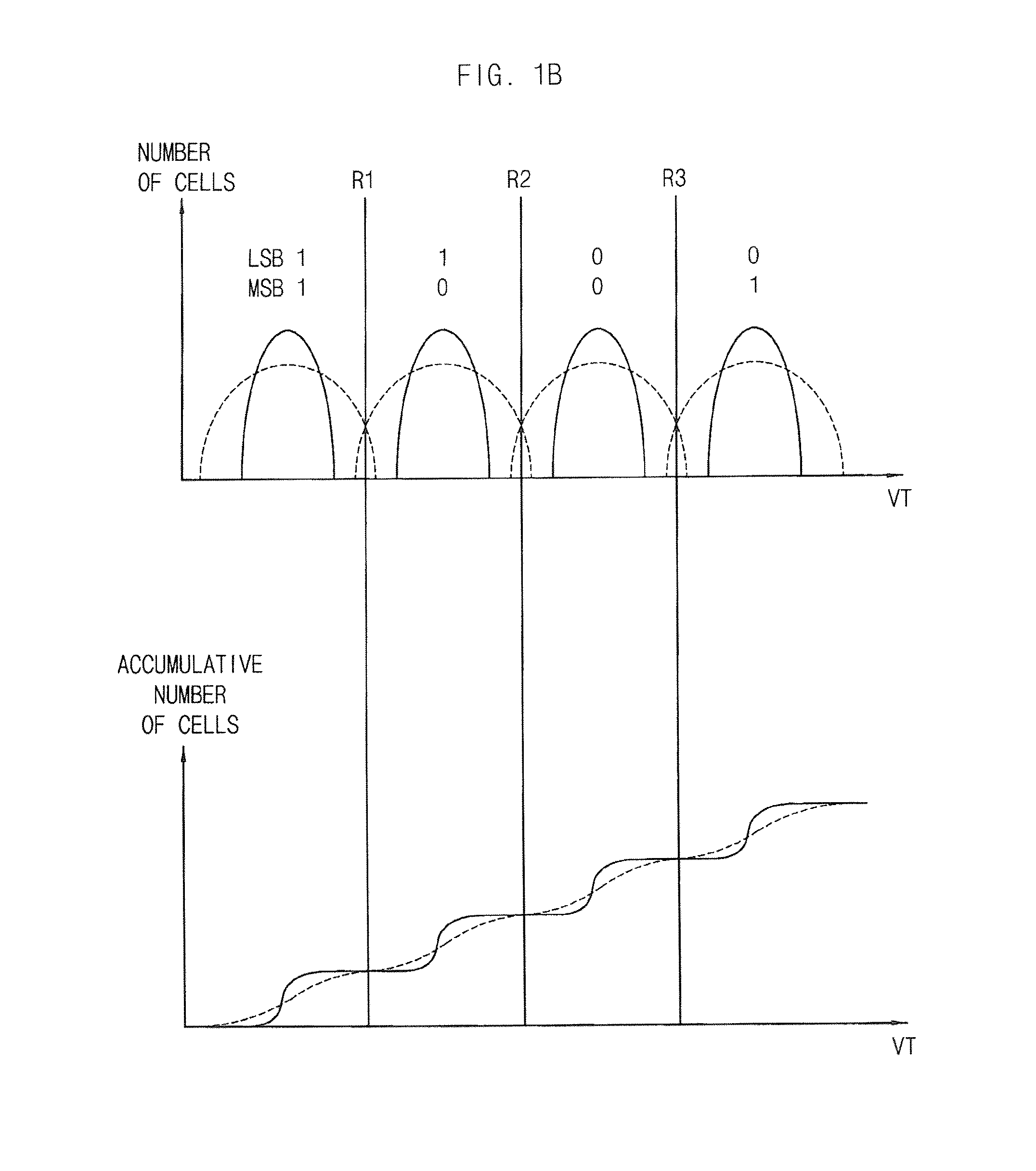
[0031]FIG. 1A is a diagram illustrating an example of a threshold voltage distribution of a memory cell in a MLC NAND flash memory device. FIG. 1B is a diagram illustrating an example of an altered threshold voltage distribution of a memory cell in a MLC NAND flash memory device.

[0032]Referring to FIG. 1A, each memory cell of the MLC NAND flash memory device may store 2-bit data including a lower-order bit and a higher-order bit. Here, the lower-order bit of MLC refers a least significant bit (LSB), and the higher-order bit of MLC refers a most significant bit (MSB). The memory cell of the MLC NAND flash me...


PUM


Abstract

A method of adjusting read voltages for a NAND flash memory device includes an operation of reading first page data from a first page corresponding to a paired page of a second page, an operation of simultaneously changing the first test read voltage and the third test read voltage to read second page data from a second page, an operation of performing a bitwise operation on the first page data and the second page data an operation of counting a number of memory cells corresponding to a first threshold voltage state and a fourth threshold voltage state by using a result of the bitwise operation, and an operation of setting a first read voltage and a third read voltage as a voltage corresponding to a section in which a change in the number of memory cells is a lowest value.

Description

BACKGROUND[0001]1. Technical Field[0002]Example embodiments relate generally to a nonvolatile memory device. More particularly, embodiments of the present inventive concept relate to a method of adjusting read voltages for a NAND flash memory device.[0003]2. Description of the Related Art[0004]A NAND flash memory device can store data by injecting an electric charge into a floating gate and read the stored data at a time when requested. The NAND flash memory device includes a plurality of memory cells. Each memory cell stores one-bit data or multi-bit data. In the single-level cell (SLC) NAND flash memory device, each memory cell corresponds to one of two threshold voltage states to store one-bit data. In contrast, in the multi-level cell (MLC) NAND flash memory device, each memory cell corresponds to one of four threshold voltage states to store 2-bit data. Further, in the triple-level cell (TLC) NAND flash memory device, each memory cell corresponds to one of eight threshold volta...

Claims


Application Information

Patent Timeline
Patent Type & Authority Patents(United States)
IPC IPC(8): G11C16/34G11C11/56G11C16/26
CPCG11C11/5642G11C16/26G11C16/3404
Inventor HAN, SEUNG-HYUNHWANG, SUN-MO
Owner THE AIO
Why Eureka
Try Eureka