Devices and methods related to packaging of radio-frequency devices on ceramic substrates

a technology of radio frequency devices and ceramic substrates, applied in semiconductor devices, semiconductor/solid-state device details, electrical apparatus, etc., can solve problems such as degrading the performance of wireless devices

Active Publication Date: 2017-02-07
SKYWORKS SOLUTIONS INC
View PDF5 Cites 3 Cited by
  • Summary
  • Abstract
  • Description
  • Claims
  • Application Information

AI Technical Summary

Benefits of technology

[0008]In some embodiments, the die can be configured as a flip-chip device. The packaged electronic device can further include an underfill implemented between the flip-chip device and the ceramic substrate. The underfill can include an edge profile configured to provide an angled transition between side walls of the flip-chip device and the surface of the ceramic substrate. The angled transition profile of the underfill can be configured to facilitate improved coverage of the conformal conductive coating between the flip-chip device and the ceramic substrate.
[0014]In some implementations, the present disclosure relates to a method for fabricating a packaged radio-frequency (RF) module. The method includes forming or providing a ceramic substrate configured to receive one or more components. The ceramic substrate includes a conductive layer in electrical contact with a ground plane. The method further includes mounting a die on a surface of the ceramic substrate, with the die including an integrated circuit. The method further includes forming a conformal conductive coating over the die and in electrical contact with the conductive layer to thereby provide shielding functionality for the die.

Problems solved by technology

Electromagnetic (EM) fields can be generated from or have an undesirable effect on a region of a radio-frequency (RF) device such as an RF module.
Such an EM interference (EMI) can degrade the performance of wireless devices that use such an RF module.

Method used


Image

  • Devices and methods related to packaging of radio-frequency devices on ceramic substrates
  • Devices and methods related to packaging of radio-frequency devices on ceramic substrates
  • Devices and methods related to packaging of radio-frequency devices on ceramic substrates

Examples


Embodiment Construction

[0029]The headings provided herein, if any, are for convenience only and do not necessarily affect the scope or meaning of the claimed invention.

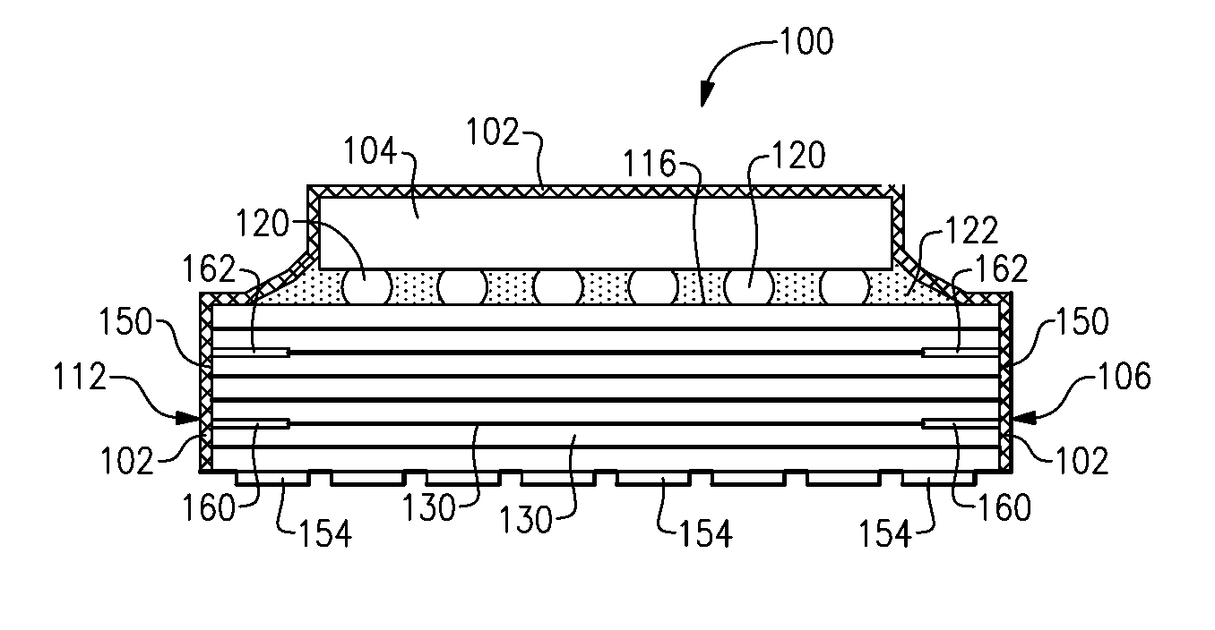
[0030]Disclosed herein are various examples of how radio-frequency (RF) devices such as flip-chip die can be mounted on a packaging substrate such as a ceramic substrate and be shielded. Although described in the context of flip-chip die, it will be understood that one or more features of the present disclosure can be implemented in other applications, including those involving non-flip-chip die. It will also be understood that one or more features of the present disclosure can also be implemented in other types of non-ceramic substrates.

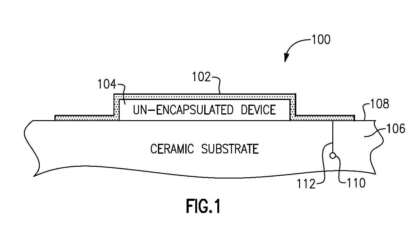
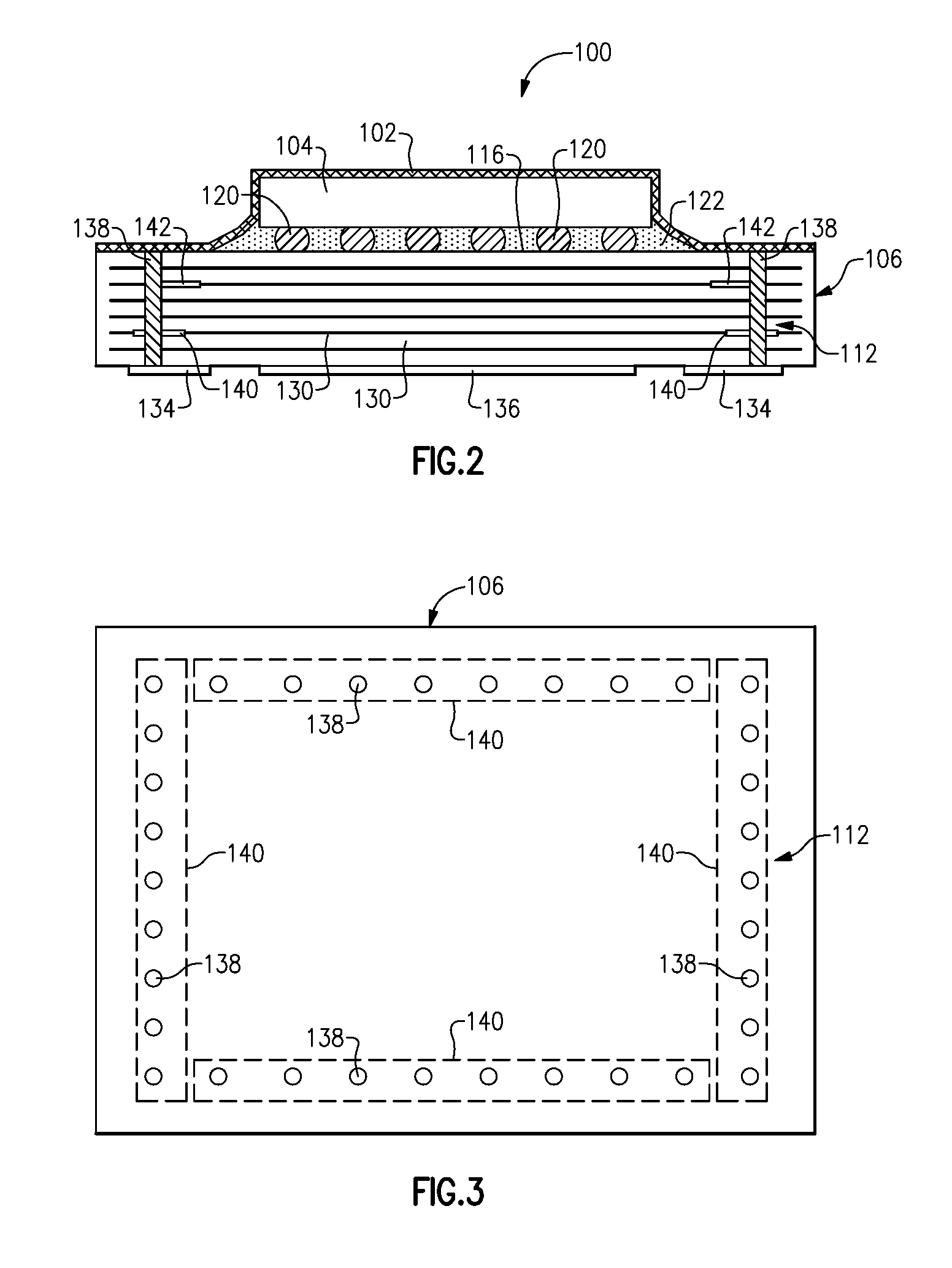
[0031]FIG. 1 shows an example of a shielded packaged device 100 that includes an un-encapsulated device 104 mounted on a ceramic substrate 106. As described herein, such an un-encapsulated device can be, for example, a flip-chip. As described herein, such a flip-chip 104 mounted on the ceramic substrate 106...


PUM

PropertyMeasurementUnit
heightaaaaaaaaaa
conductiveaaaaaaaaaa
radio-frequency aaaaaaaaaa

Abstract

Devices and methods related to packaging of radio-frequency (RF) devices on ceramic substrates. In some embodiments, a packaged electronic device can include a ceramic substrate configured to receive one or more components. The ceramic substrate can include a conductive layer in electrical contact with a ground plane. The packaged electronic device can further include a die having an integrated circuit and mounted on a surface of the ceramic substrate. The packaged electronic device can further include a conformal conductive coating implemented over the die to provide shielding functionality. The packaged electronic device can further include an electrical connection between the conformal conductive coating and the conductive layer.

Description

CROSS-REFERENCE TO RELATED APPLICATION(S)[0001]This application claims priority to U.S. Provisional Application No. 61 / 900,394 filed Nov. 5, 2013, entitled DEVICES AND METHODS RELATED TO PACKAGING OF RADIO-FREQUENCY DEVICES ON CERAMIC SUBSTRATES, the disclosure of which is hereby expressly incorporated by reference herein in its entirety.BACKGROUND[0002]Field[0003]The present disclosure generally relates to shielding of packaged radio-frequency (RF) modules.[0004]Description of the Related Art[0005]Electromagnetic (EM) fields can be generated from or have an undesirable effect on a region of a radio-frequency (RF) device such as an RF module. Such an EM interference (EMI) can degrade the performance of wireless devices that use such an RF module. Some RF modules can be provided with EM shields to address such performance issues associated with EMI.SUMMARY[0006]According to some implementations, the present disclosure relates to a packaged electronic device that includes a ceramic su...

Claims


Application Information

Patent Timeline
Patent Type & Authority Patents(United States)
IPC IPC(8): H04B1/38H01L21/67H01L23/15H01L21/48H05K9/00H01L23/31H01L23/00H01L23/06
CPCH04B1/38H01L21/481H01L23/15H05K9/0026H01L21/67236H01L23/06H01L23/3121H01L24/94H01L2224/16225H01L2224/32225H01L2224/73204Y10T29/49128H01L2924/00H01L2924/15313H01L2924/3025H01L21/32051H01L21/563H01L21/78H01L23/3142H01L23/49822H01L23/49827H01L23/49838H01L23/49894H01L23/552H01L24/17H01L24/81H01L24/97H01L2224/16055H01L2224/16113H01L2224/16227H01L2224/1713H01L2224/17179H01L2924/1421H01L2924/19041H01L2924/19042H01L2924/19043
Inventor LOBIANCO, ANTHONY JAMESCHEN, HOWARD E.WHITEFIELD, DAVID SCOTT
Owner SKYWORKS SOLUTIONS INC
Why Eureka
Try Eureka