Method of fabricating SOI wafer by ion implantation

a technology of ion implantation and bonded wafer, which is applied in the direction of basic electric elements, electrical apparatus, semiconductor devices, etc., can solve the problems of layer degrading uniformity and damage layer on the surface, and achieves low bmd density, smooth surface roughness, and low bmd density.

Active Publication Date: 2017-08-15
SHIN-ETSU HANDOTAI CO LTD
View PDF20 Cites 2 Cited by
  • Summary
  • Abstract
  • Description
  • Claims
  • Application Information

AI Technical Summary

Benefits of technology

[0027]According to the inventive method of manufacturing a bonded wafer, the RTA is performed such that the retention temperature is higher at the beginning and lower at the end, and the sacrificial oxidation process is subsequently performed. The invention can thereby produce a bonded wafer having a low BMD density and smoothed surface roughness. This bonded wafer having a low BMD density is prevented from severely deforming even when being subjected to a heat treatment in a device process, and hardly causes a failure of misalignment of patterns in photolithography.

Problems solved by technology

The SOI wafer after the separation, however, has a damage layer on its surface due to the ion implantation.
Even though the implantation of ions such as hydrogen ions and the separation can achieve the uniformity of the thickness of the SOI layer to a certain extent, a polishing process including such a mechanical factor performed on the SOI layer degrades this uniformity because of nonuniform polishing stock removal.

Method used


Image

  • Method of fabricating SOI wafer by ion implantation
  • Method of fabricating SOI wafer by ion implantation
  • Method of fabricating SOI wafer by ion implantation

Examples


example 1

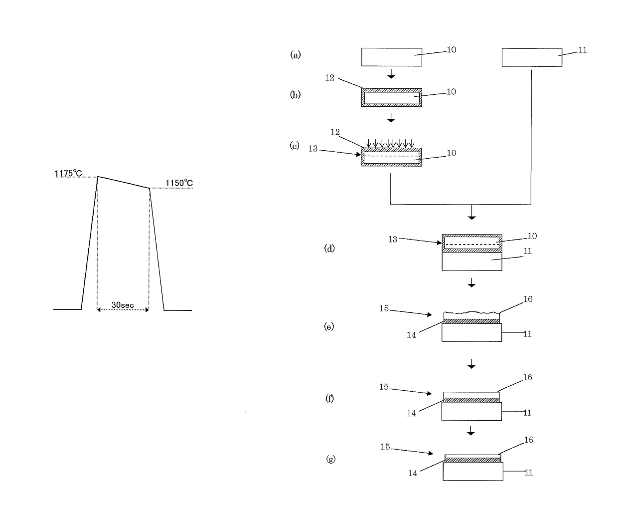
[0059]A silicon single crystal wafer (having a diameter of 300 mm and a crystal orientation of ) with no crystal originated particle (COP) was prepared as a bond wafer. After a 190-nm oxide film was grown on this bond wafer, 5×10¹⁶ atoms / cm2 of H+ ions were implanted at an acceleration energy of 50 keV with an ion implantation apparatus to form a layer of the implanted ions.

[0060]A silicon single crystal wafer (having no oxide film, a diameter of 300 mm, and a crystal orientation of ) with an oxygen concentration of 22.4 ppma (ASTM'79) was prepared as a base wafer, and brought into close contact with the bonding surface of the implantation surface of the bond wafer. A heat treatment was then performed on these contacting wafers at temperatures ranging from a start temperature of 200° C. to a maximum temperature of 500° C. with a batch type of horizontal heat treatment furnace so that the bond wafer was separated along the layer of the implanted ions. An SOI layer was thereby formed ...

example 2

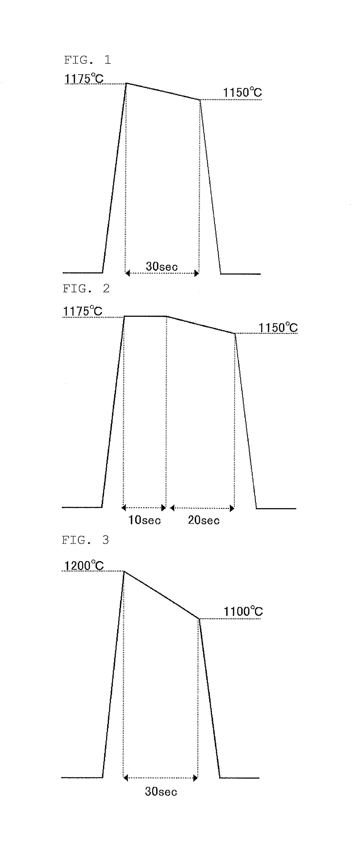
[0063]The bond wafer was separated along the layer of implanted ions under the same conditions as example 1 so that the SOI layer was formed on the base wafer. With a single-wafer-processing type of RTA apparatus, a surface of this SOI layer was subjected to RTA under a mixed gas atmosphere of 50% hydrogen and 50% argon; this RTA included rapid temperature increase (30° C. / second), rapid temperature decrease (30° C. / second), and temperature retention period interposed therebetween; the temperature at the beginning of this retention was 1175° C.; the retention period was first continued for 10 second at 1175° C. and then for 20 seconds while the temperature was monotonously decreased; and the temperature at the end of this retention was 1150° C. FIG. 2 shows the temperature profile of this heat treatment. An oxide film was then grown on the SOI surface by pyrogenic oxidation at 900° C. and a heat treatment at 1050° C. under an argon gas containing 1% oxygen in a batch type of vertica...

example 3

[0065]The bond wafer was separated along the layer of implanted ions under the same conditions as example 1 so that the SOI layer was formed on the base wafer. With a single-wafer-processing type of RTA apparatus, a surface of this SOI layer was subjected to RTA under a mixed gas atmosphere of 50% hydrogen and 50% argon; this RTA included rapid temperature increase (30° C. / second), rapid temperature decrease (30° C. / second), and temperature retention period interposed therebetween; the temperature at the beginning of this retention was 1200° C.; the retention period was continued for 30 seconds while the temperature was monotonously decreased; and the temperature at the end of this retention was 1100° C. FIG. 3 shows the temperature profile of this heat treatment. An oxide film was then grown on the SOI surface by pyrogenic oxidation at 900° C. and a heat treatment at 1050° C. under an argon gas containing 1% oxygen in a batch type of vertical heat treatment furnace. The oxide film ...


PUM

PropertyMeasurementUnit
retention end temperatureaaaaaaaaaa

Abstract

The present invention provides a method of manufacturing a bonded wafer, including performing RTA under an atmosphere containing hydrogen on a bonded wafer after separating the bond wafer constituting the bonded wafer, and subsequently performing a sacrificial oxidation process to reduce the thickness of the thin film, wherein the RTA is performed under conditions of a retention start temperature of more than 1150° C. and a retention end temperature of 1150° C. or less. The invention can inhibit the BMD density from increasing and sufficiently flatten the surface of a thin film when the thin film of the bonded wafer is flattened and thinned by the combination of the RTA and sacrificial oxidation processes.

Description

TECHNICAL FIELD[0001]The present invention relates to a method of manufacturing a bonded wafer by an ion implantation separation method.BACKGROUND ART[0002]A method of separating ions-implanted wafers after bonding to manufacture SOI wafers, i.e., an ion implantation separation method (a technique also referred to as the Smart Cut method (registered trademark)), has attracted attention as a method of manufacturing silicon on insulator (SOI) wafers, particularly a method of manufacturing thin-SOI wafers that enable improvement in performance of advanced integrated circuits.[0003]This ion implantation separation method is a technique to form an SOI wafer (See Patent Literature 1) in the following manner: an oxide film (an insulator film) is formed on at least one of two silicon wafers; gas ions such as hydrogen ions or rare gas ions are implanted from a front surface of one of the silicon wafers (a bond wafer) to form a micro bubble layer (an enclosed layer) in the interior of the waf...

Claims


Application Information

Patent Timeline
Patent Type & Authority Patents(United States)
IPC IPC(8): H01L21/30H01L21/683H01L21/18H01L21/02H01L21/324H01L21/265H01L27/12H01L21/762
CPCH01L21/76254H01L21/02329H01L21/187H01L21/265H01L21/324H01L21/3247H01L21/6835H01L27/1203
Inventor ISHIZUKA, TORUKOBAYASHI, NORIHIRO
Owner SHIN-ETSU HANDOTAI CO LTD
Why Eureka
Try Eureka