Semiconductor packages having an electric device with a recess

a technology of semiconductor devices and electric devices, applied in the field of semiconductor devices, can solve problems such as reliability problems, distortions or delaminations within the package, reliability problems of semiconductor devices,

Active Publication Date: 2017-11-21
STMICROELECTRONICS INT NV
View PDF7 Cites 0 Cited by
  • Summary
  • Abstract
  • Description
  • Claims
  • Application Information

AI Technical Summary

Benefits of technology

[0005]Embodiments are directed to a package that includes an electric device having a recess. In one embodiment, the recess is substantially filled with adhesive material improving adhesion between the electric device and a substrate of the package while at the same time allowing for lower adhesive fillets. In another embodiment, the electric device is a sensor and the recess reduces signal drift of the sensor caused by thermal expansion of the package.

Problems solved by technology

Various issues are known to cause reliability problems in semiconductor devices.
For instance, heat generated by the operation of a semiconductor device that remains in the package can cause reliability issues.
Some of the different materials may have different coefficients of thermal expansion (CTE), and thus heat that remains in the package can result in varying thermal expansion rates thereby causing distortions or delamination within the package.

Method used


Image

  • Semiconductor packages having an electric device with a recess
  • Semiconductor packages having an electric device with a recess
  • Semiconductor packages having an electric device with a recess

Examples


Embodiment Construction

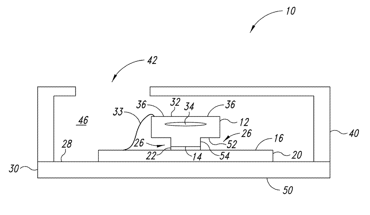
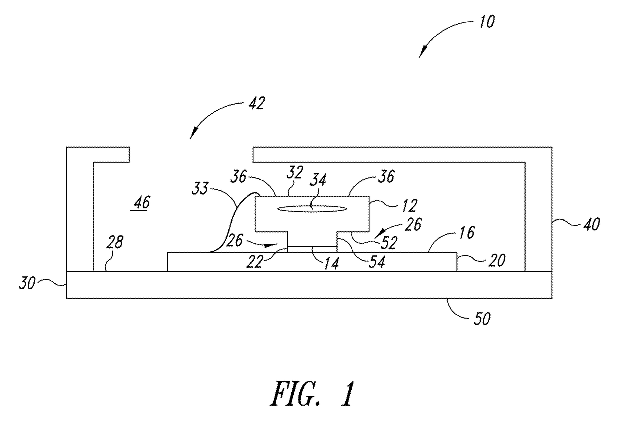
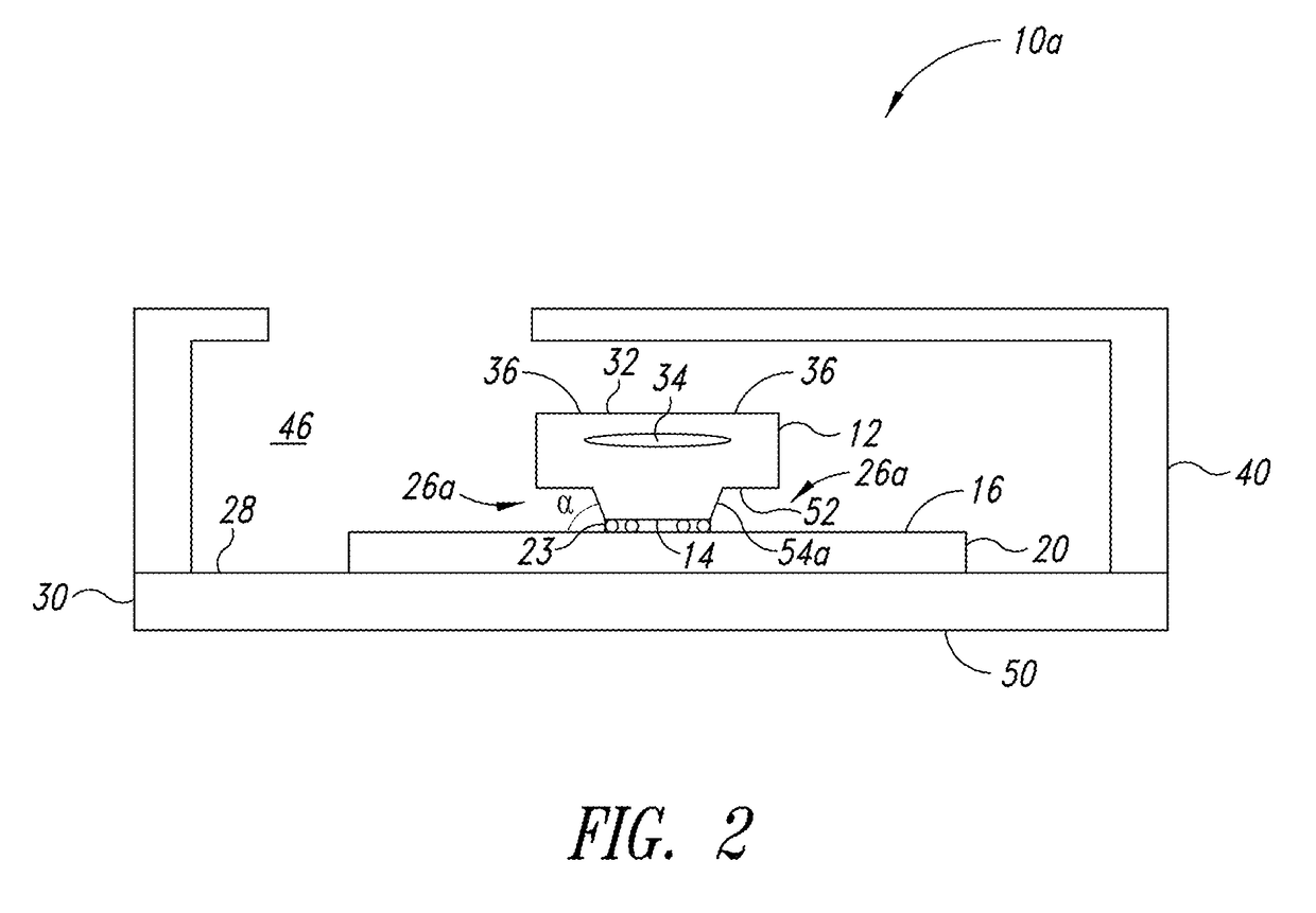
[0012]FIG. 1 shows a side view of a package 10 according to one embodiment of the present disclosure. The package 10 includes an electric device, such as a sensor 12, having a back surface 14 secured to an upper surface 16 of an integrated circuit 20 by an adhesive 22, such as glue or tape. The back surface 14 of the sensor 12 includes a recess 26, the details of which will be described below. The integrated circuit 20 is secured to an upper surface 28 of a substrate 30, thereby fixing the sensor 12 relative to the substrate 30.

[0013]In FIG. 1, the sensor 12 is a pressure sensor. However, the sensor 12 may be any sensor, such as a micro-electromechanical sensor (MEMS), or any electric device. In the illustrated embodiment, the pressure sensor 12 includes a membrane 32 that is located above a cavity 34 suspending the membrane 32. At the outer edges of the membrane 32 are transducer elements 36, such as piezoresistors, which are configured to measure deflections of the membrane 32 and...


PUM


Abstract

Embodiments are directed to a package that includes an electric device having a recess. In one embodiment, the electric device is a sensor and the recess reduces signal drift of the sensor caused by thermal expansion of the package. In another embodiment, the recess is substantially filled with adhesive material, thus increasing adhesion between the electric device and a substrate of the package while at the same time allowing for lower adhesive fillets.

Description

BACKGROUND[0001]Technical Field[0002]Embodiments of the present disclosure are related to semiconductor packages that includes at least one electric device.[0003]Description of the Related Art[0004]Reliability of semiconductor devices is of significant importance. Various issues are known to cause reliability problems in semiconductor devices. For instance, heat generated by the operation of a semiconductor device that remains in the package can cause reliability issues. One reason for this is that packages are formed of varying types of materials. Some of the different materials may have different coefficients of thermal expansion (CTE), and thus heat that remains in the package can result in varying thermal expansion rates thereby causing distortions or delamination within the package.BRIEF SUMMARY[0005]Embodiments are directed to a package that includes an electric device having a recess. In one embodiment, the recess is substantially filled with adhesive material improving adhes...

Claims


Application Information

Patent Timeline
Patent Type & Authority Patents(United States)
IPC IPC(8): H01L23/02B81B7/00H01L23/00H01L21/78H01L23/053
CPCH01L21/78B81B7/0048H01L24/32H01L24/83H01L2924/16151H01L2924/12042H01L2924/10158H01L2924/10157H01L2924/00014H01L2224/83007H01L2224/73265H01L2224/48091H01L2224/32058H01L2224/29198H01L2224/29101H01L2224/27013H01L2224/16225H01L23/053H01L24/13H01L24/29H01L24/48H01L2224/13101H01L2224/45099H01L2924/014H01L2924/00H01L27/14618H01L2224/48227H01L2924/00012
Inventor GOH, KIM-YONGZHANG, XUERENMA, YIYI
Owner STMICROELECTRONICS INT NV
Why Eureka
Try Eureka