Methods for selective etching of a silicon material using HF gas without nitrogen etchants

a selective etching and silicon material technology, applied in the direction of basic electric elements, electrical equipment, electric discharge tubes, etc., can solve the problems of deteriorating device performance and electrical properties of the device structure, void space, and other associated defects, and achieve high selectivity

Inactive Publication Date: 2017-11-28
APPLIED MATERIALS INC
View PDF14 Cites 95 Cited by
  • Summary
  • Abstract
  • Description
  • Claims
  • Application Information

AI Technical Summary

Problems solved by technology

Reliably producing sub-half micron and smaller features is one of the key technology challenges for next generation very large scale integration (VLSI) and ultra large-scale integration (ULSI) of semiconductor devices.
However, as the limits of circuit technology are pushed, the shrinking dimensions of VLSI and ULSI technology have placed additional demands on processing capabilities.
Typically, conventional etchants have low selectivity to etch one material over another material present in the structure, such as gate dielectric, gate electrode and / or underlying materials in a gate structure, thereby leaving void space, also known as silicon recess, foot, or other associated defects on the interface of different materials.
Low selectivity of the etchants between different materials often result in etching profile deformation, specifically forming defects on sidewalls, corners, or bottom the substrate surface which may deteriorate device performance and electrical properties of the device structure.

Method used


Image

  • Methods for selective etching of a silicon material using HF gas without nitrogen etchants
  • Methods for selective etching of a silicon material using HF gas without nitrogen etchants
  • Methods for selective etching of a silicon material using HF gas without nitrogen etchants

Examples


Embodiment Construction

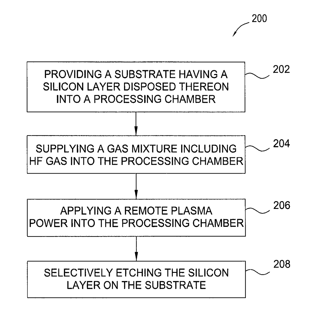
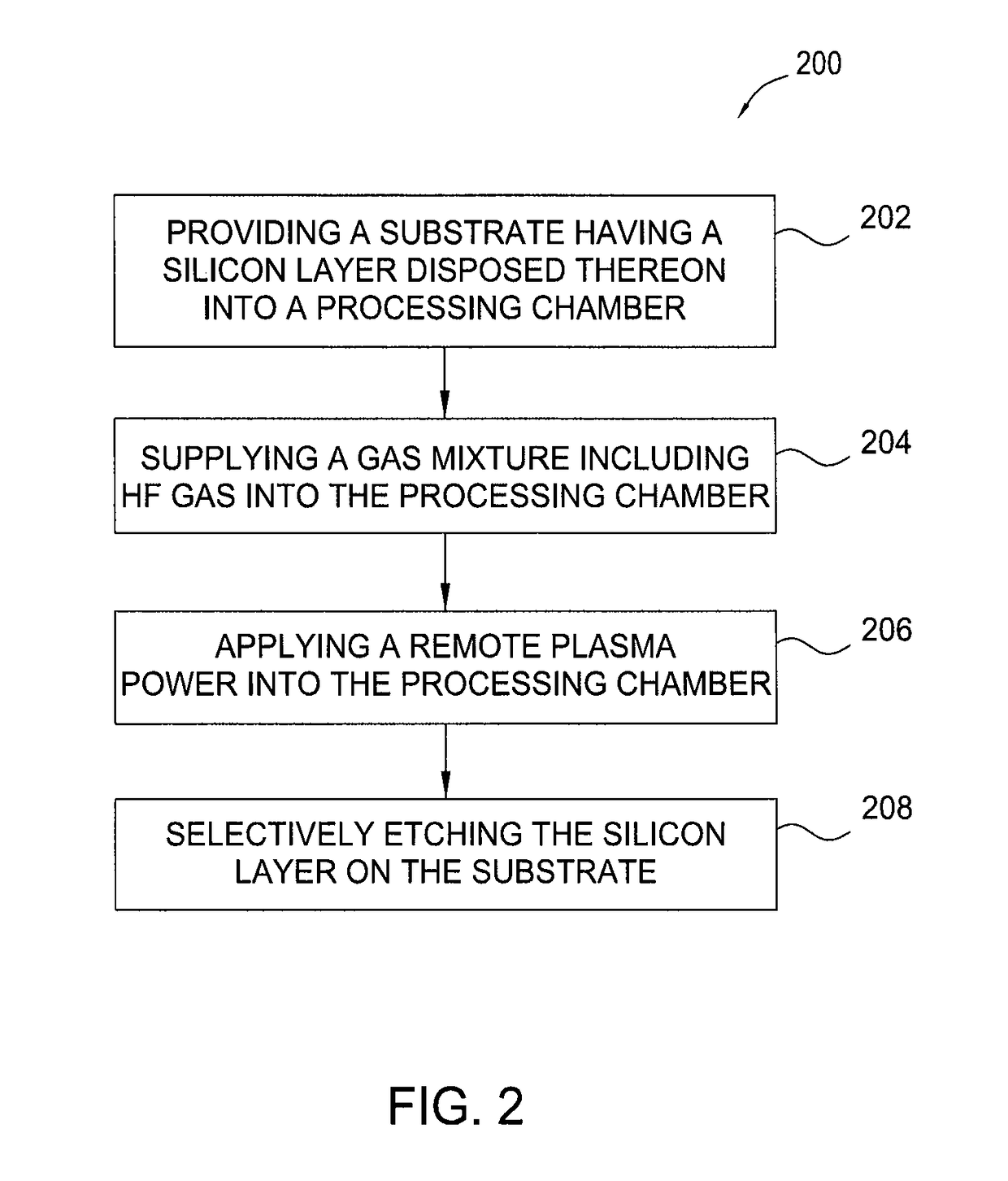
[0019]Embodiments of the invention generally relate to methods and apparatus for etching a silicon material from a device structure disposed on a substrate. In one example, the method includes etching a silicon material from a remote plasma source including HF etchants with optional nitrogen free hydrogen containing gas, such as H2 gas. The HF etchants along with the optional nitrogen free hydrogen containing gas, such as H2 gas, predominantly remove the silicon material from the substrate without attacking other materials included in the structure formed on the substrate, thus providing a selective etching process to etch the silicon material. The HF etchants may be supplied from a remote plasma source so as to gently remove the silicon material without over aggressively attacking the materials disposed on the substrate. The etching gas excludes nitrogen etchants during the etching process.

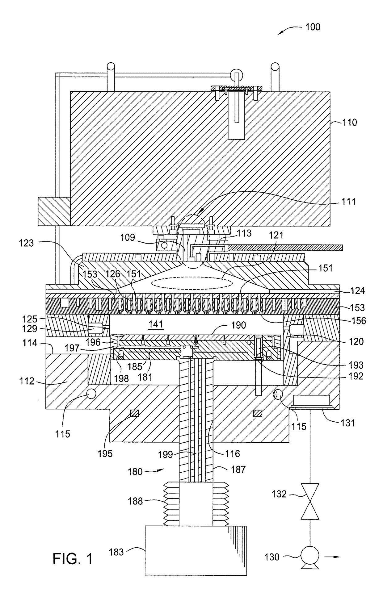
[0020]FIG. 1 is a cross sectional view of an illustrative processing chamber 100 suitable for...


PUM

PropertyMeasurementUnit
temperatureaaaaaaaaaa

Abstract

The present disclosure provides methods for etching a silicon material in a device structure in semiconductor applications. In one example, a method for etching features in a silicon material includes performing a remote plasma process formed from an etching gas mixture including HF gas without nitrogen etchants to remove a silicon material disposed on a substrate.

Description

CROSS-REFERENCE TO RELATED APPLICATIONS[0001]This application claims benefit of U.S. Provisional Application Ser. No. 62 / 269,695 filed Dec. 18, 2015, which is incorporated by reference in its entirety.BACKGROUND[0002]Field[0003]Embodiments of the present invention generally relate to methods for selectively etching a silicon material disposed on a substrate for semiconductor manufacturing applications.[0004]Description of the Related Art[0005]Reliably producing sub-half micron and smaller features is one of the key technology challenges for next generation very large scale integration (VLSI) and ultra large-scale integration (ULSI) of semiconductor devices. However, as the limits of circuit technology are pushed, the shrinking dimensions of VLSI and ULSI technology have placed additional demands on processing capabilities. Reliable formation of gate structures on the substrate is important to VLSI and ULSI success and to the continued effort to increase circuit density and quality o...

Claims


Application Information

Patent Timeline
Patent Type & Authority Patents(United States)
IPC IPC(8): H01L21/3065H01L21/308
CPCH01L21/3081H01L21/3065H01J37/32357H01L21/31116H01L21/31122H01L21/32137
Inventor INGLE, NITIN K.WANG, ANCHUANLI, ZIHUIKOROLIK, MIKHAIL
Owner APPLIED MATERIALS INC
Why Eureka
Try Eureka