Pattern weakness and strength detection and tracking during a semiconductor device fabrication process

a semiconductor device and fabrication process technology, applied in semiconductor/solid-state device testing/measurement, instruments, image enhancement, etc., can solve the problems of difficulty in evaluating and examining anomalies that may be present, the number of defects on the wafers within the lot,

Active Publication Date: 2017-12-19
ANCHOR SEMICON
View PDF24 Cites 8 Cited by
  • Summary
  • Abstract
  • Description
  • Claims
  • Application Information

AI Technical Summary

Problems solved by technology

Generally, these inspections report a number of defects on the wafers within the lot.
Due to the diversity of features in an image and the large volume of images being generated, it can be challenging to evaluate and examine anomalies that may be present.

Method used


Image

  • Pattern weakness and strength detection and tracking during a semiconductor device fabrication process
  • Pattern weakness and strength detection and tracking during a semiconductor device fabrication process
  • Pattern weakness and strength detection and tracking during a semiconductor device fabrication process

Examples


Embodiment Construction

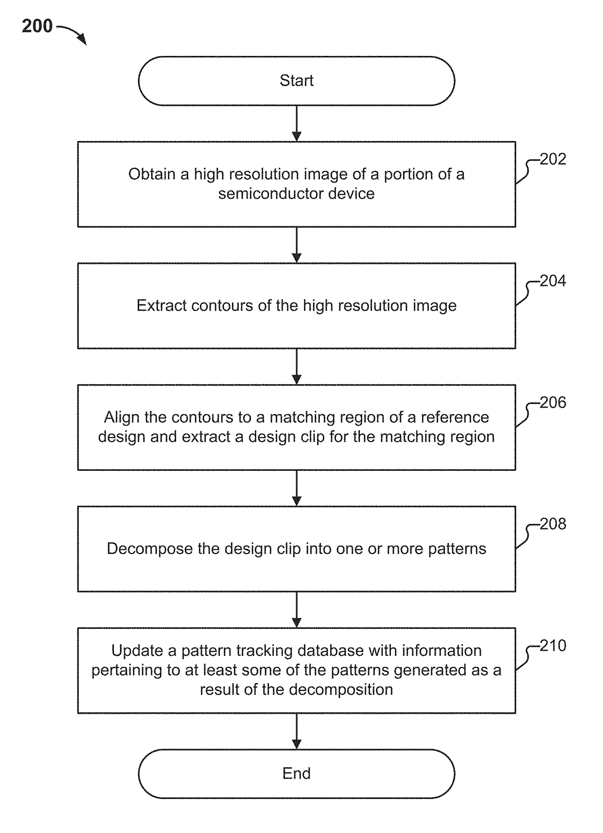
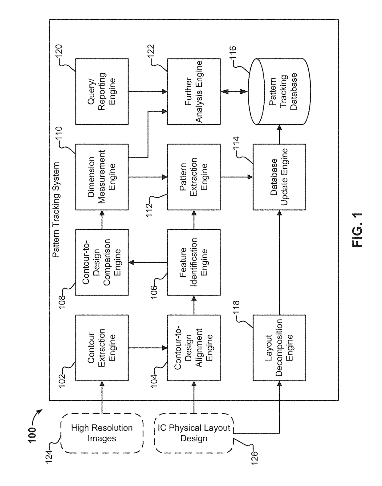
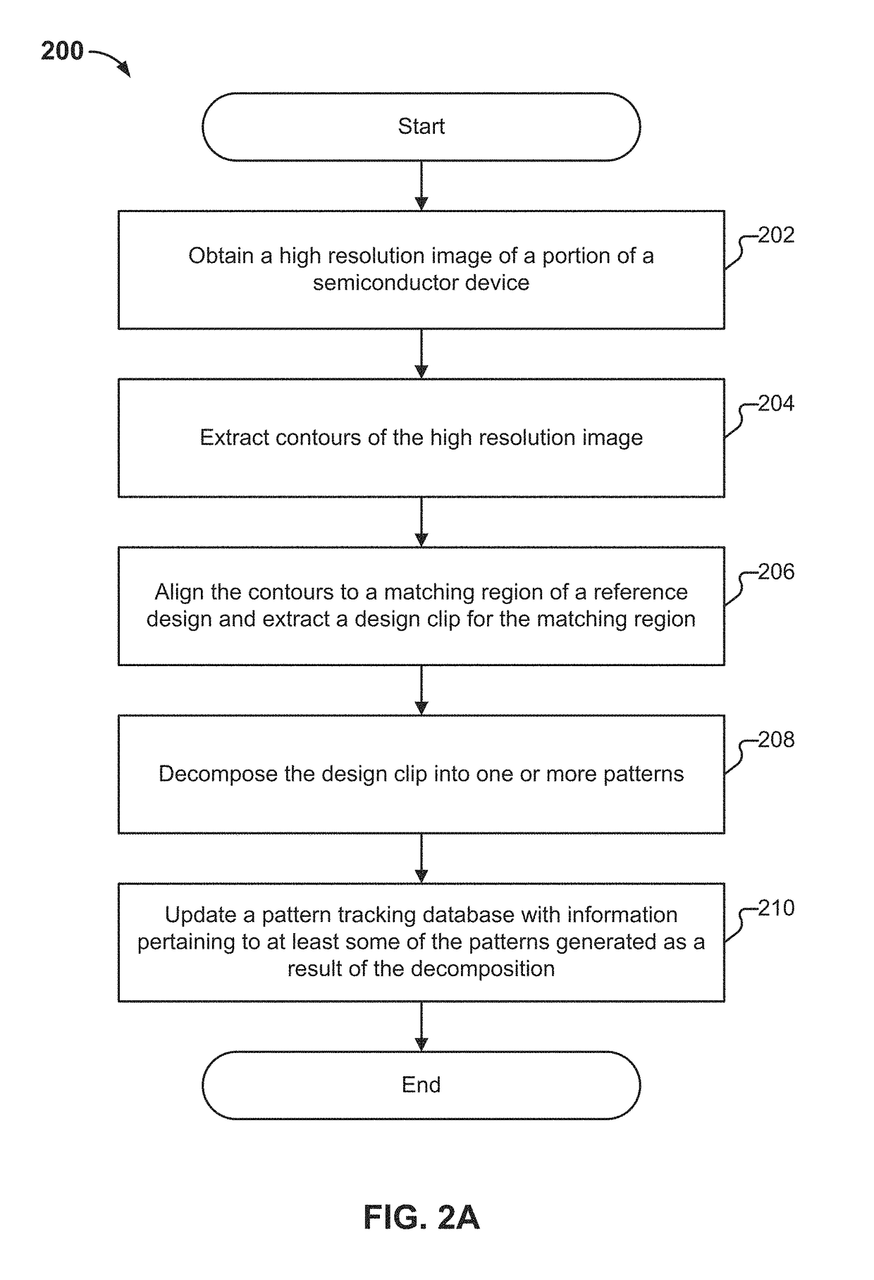
[0022]The invention can be implemented in numerous ways, including as a process; an apparatus; a system; a composition of matter; a computer program product embodied on a computer readable storage medium; and / or a processor, such as a processor configured to execute instructions stored on and / or provided by a memory coupled to the processor. In this specification, these implementations, or any other form that the invention may take, may be referred to as techniques. In general, the order of the steps of disclosed processes may be altered within the scope of the invention. Unless stated otherwise, a component such as a processor or a memory described as being configured to perform a task may be implemented as a general component that is temporarily configured to perform the task at a given time or a specific component that is manufactured to perform the task. As used herein, the term ‘processor’ refers to one or more devices, circuits, and / or processing cores configured to process da...


PUM


Abstract

Tracking patterns during a semiconductor fabrication process includes: obtaining an image of a portion of a fabricated device; extracting contours of the portion of the fabricated device from the obtained image; aligning the extracted contour to a matching section of a reference design; decomposing the matching section of the reference design into one or more patterns; and updating a pattern tracking database with information pertaining to at least one pattern in the one or more patterns generated as a result of the decomposition.

Description

CROSS REFERENCE TO OTHER APPLICATIONS[0001]This application claims priority to U.S. Provisional Patent Application No. 62 / 146,572 entitled PATTERN WEAKNESS AND STRENGTH DETECTION AND TRACKING DURING A SEMICONDUCTOR DEVICE FABRICATION PROCESS filed Apr. 13, 2015 which is incorporated herein by reference for all purposes.BACKGROUND OF THE INVENTION[0002]During the semiconductor device fabrication process, high speed, low resolution wafer inspections (e.g., Bright Field, Dark Field, etc.) are performed on selected wafers from a fabrication lot. Generally, these inspections report a number of defects on the wafers within the lot. Out of the reported detects, a small subset (e.g., a sub-sample) of the defects are selected for review and defect-type classification. Classification can be done by capturing a high-resolution image of each sampled defect, examining the image to determine the type of defect present, then assigning an appropriate classification code to the defect. High-resoluti...

Claims


Application Information

Patent Timeline
Patent Type & Authority Patents(United States)
IPC IPC(8): G06K9/00G06K9/62G06K9/46G06K9/52G06T7/00
CPCG06T7/001G06K9/4604G06K9/4671G06K9/6201G06K9/52G06T2207/30148G06K2009/4666G06T2207/20081G01N21/8806H01L22/20H01L22/30G01N2223/418G01N2021/8887G06F18/22
Inventor ZAFAR, KHURRAMHU, CHENMINCHEN, YEMA, YUEHSIANG, CHINGYUNCHEN, JUSTINXU, RAYMONDVIKRAM, ABHISHEKZHANG, PING
Owner ANCHOR SEMICON
Why Eureka
Try Eureka