Increased contact alignment tolerance for direct bonding

a direct bonding and alignment tolerance technology, applied in the direction of electrical equipment, semiconductor devices, semiconductor/solid-state device details, etc., can solve the problems of high defect density of hetero-epitaxial grown films, dislocation generation, debonding or cracking, and difficult optimization of process design needed to produce different functions on the same chip containing different materials

Active Publication Date: 2017-12-26
INVENSAS BONDING TECH INC
View PDF42 Cites 95 Cited by
  • Summary
  • Abstract
  • Description
  • Claims
  • Application Information

AI Technical Summary

Benefits of technology

[0024]Another object is to provide a room temperature bonding method by which different substrates or different materials on different substrates with different thermal expansion coefficients can be bonded together without generation of catastrophic stresses between the different substrates or different materials on different substrates.
[0027]A still further object is to provide a method and device whereby a reliable mechanical bond can be formed at or near room temperature and a reliable electrical contact can be subsequently formed with a simple low temperature anneal.

Problems solved by technology

To date, such hetero-epitaxial growth has realized a high density of defects in the hetero-epitaxial grown films, largely due to the mismatches in lattice constants between the non-silicon films and the substrate.
However, wafer bonding of dissimilar materials having different thermal expansion coefficients at elevated temperature introduces thermal stresses that lead to dislocation generation, debonding, or cracking.
The design of processes needed to produce different functions on the same chip containing different materials is difficult and hard to optimize.
Indeed, many of the resultant SOC chips (especially those at larger integration size) show a low yield.
However, wafer adhesive bonding usually operates at elevated temperatures and suffers from thermal stress, out-gassing, bubble formation and instability of the adhesive, leading to reduced yield in the process and poor reliability over time.
Very small bonding metal pads can be used, resulting in very low parasitic impedance and resulting reduced power and increased bandwidth capability.
Temperature, pressure and low hardness metals are typically employed and usually results in residual stresses.
It can be challenging, however, to achieve both alignment of metal features from two substrates and achieve reliable metal bonding while also directly bonding surrounding non-metal regions.

Method used


Image

  • Increased contact alignment tolerance for direct bonding
  • Increased contact alignment tolerance for direct bonding
  • Increased contact alignment tolerance for direct bonding

Examples


second embodiment

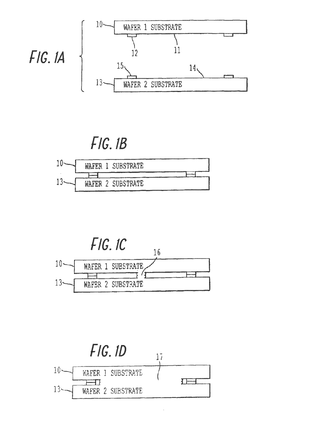
[0084]FIGS. 3A-3C are schematic drawings of a process by which two different fully processed dies are bonded. The dies are shown to have planar but uneven layer thickness, to demonstrate that the disclosed embodiments may be used in other instances other than even and planar layer thicknesses. In this process, as shown in FIG. 3A, a separate die 30 (only the oxide layer of die 30 is shown, for convenience of explanation) has metal pads 31. The die may be a silicon wafer including semiconductor devices and circuits have opposing surfaces of SiO2. Surface 32 results after a CMP operation.

[0085]As shown in FIG. 3B, vias 36 have been formed and filled with metal to connect with metal pads 31, metal interconnects 33 are formed on wafer 30 to connect with the metal in vias 36, and a layer 34 of thickness t2, of SiO2 or other insulating material is formed on wafer 30. Portions 35 of the SiO2 layer having a width w2 have been removed to expose metal pads 35. The surface of layer 34 is trea...

first embodiment

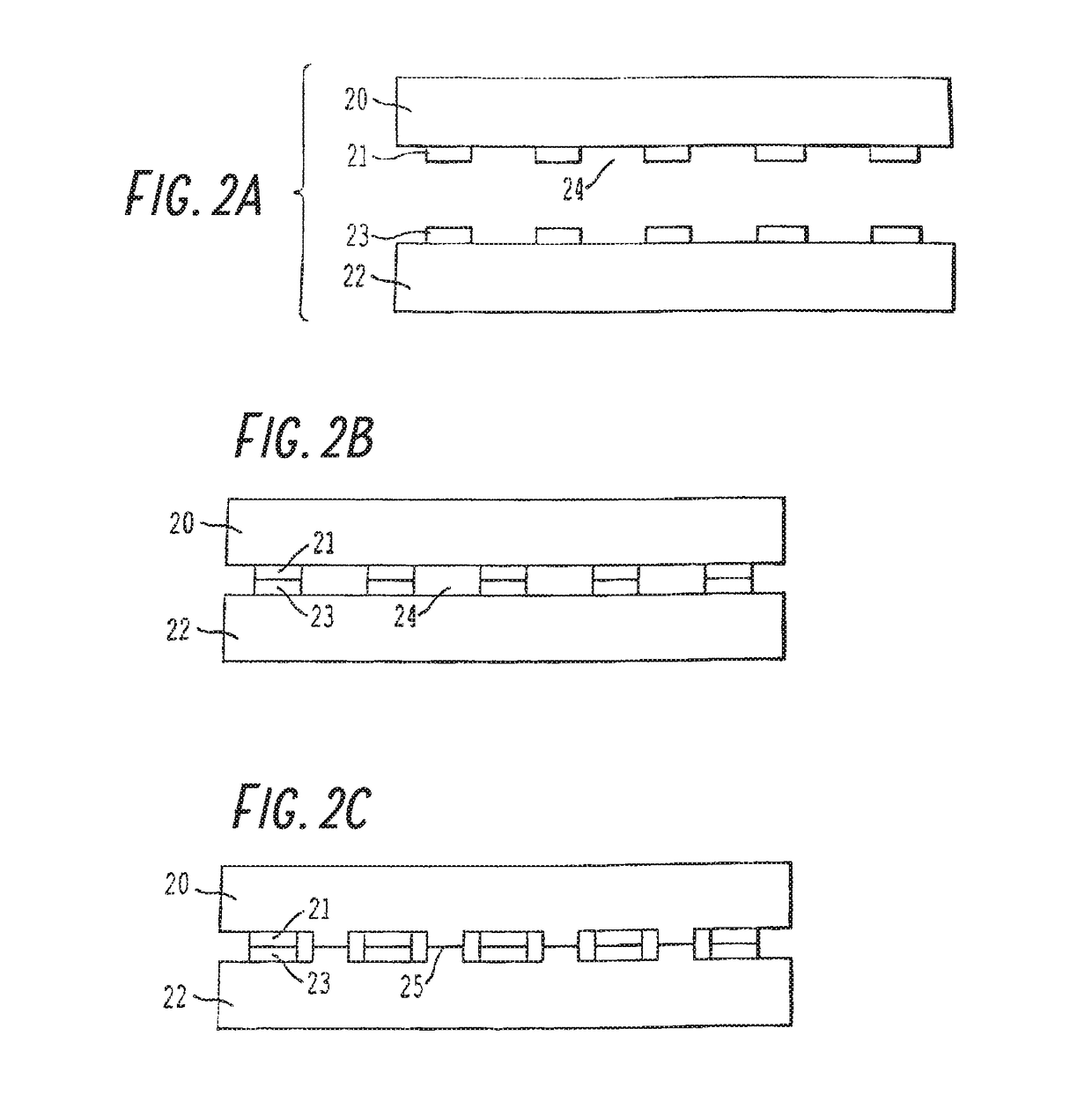
[0088]As in the first embodiment, wafer surfaces 32 and 41 including metal pads 33 and 40 contact, the contacting non-metal (e.g., semiconductor or insulator) parts of opposing wafer surfaces 32 and 41 began to form a bond at the contact points, and the bonding force increases as the contact bonding area increases. Without the presence of protruding metal pads 33 and 40, the wafers would bond across the entire wafer surface. The presence of protruding metal pads 33 and 40, while interrupting the bonding seam between the opposing wafers, does not prohibit wafer to wafer bonding. Rather, the pressure generated by the wafer-to-wafer contact in the non-metal regions translates into a force by which metal pads 33 and 40 are contacted even without any external pressure.

[0089]The method can be carried out in ambient conditions rather than being restricted to high or ultra-high vacuum (UHV) conditions. Consequently, the method is a low-cost, mass-production manufacturing technology. The siz...

third embodiment

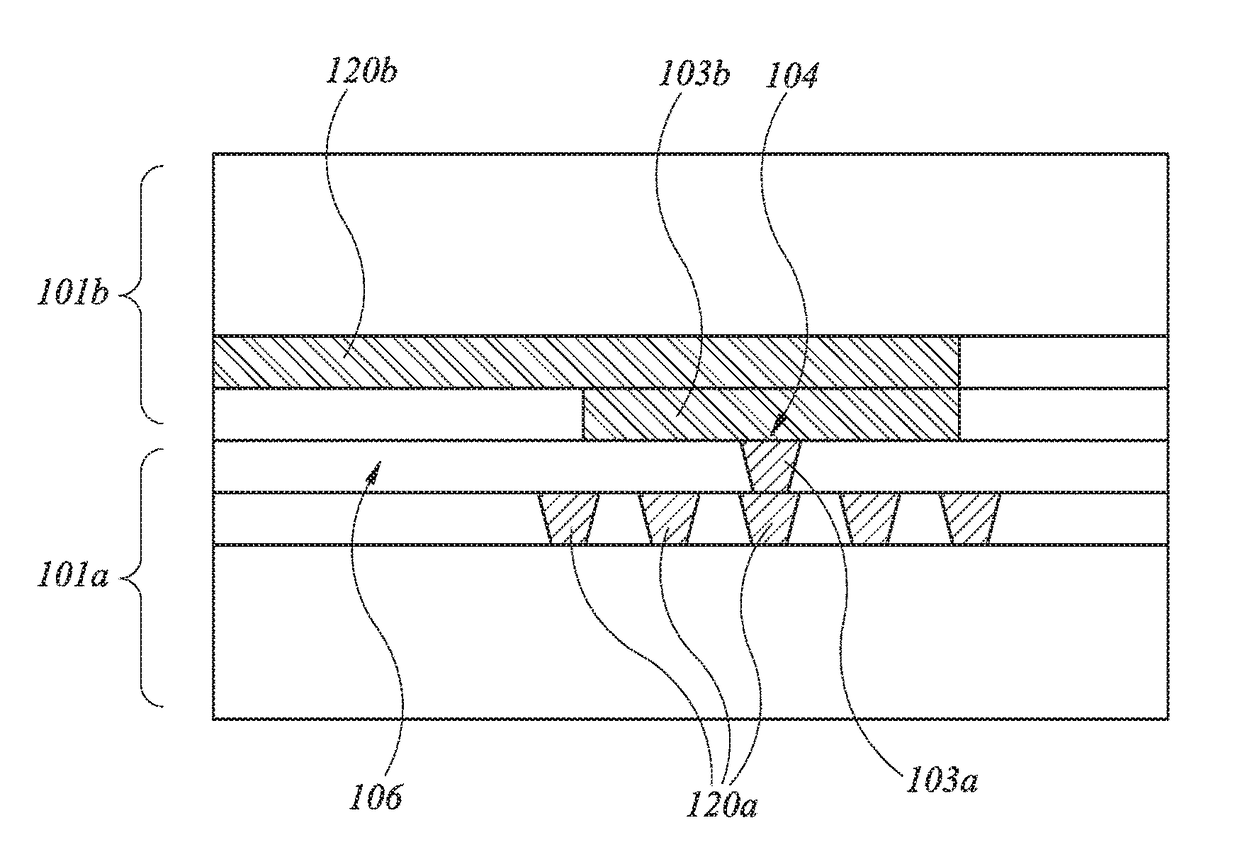
[0106]A third embodiment allows a significant increase in the metal height above the non-metal surface and / or significant reduction in non-bonded area near the metal while maintaining an acceptable electrical connection between metal portions formed on separate wafers. In this embodiment, deformation of material in the vicinity of the metal material that forms the electrical contact is designed to result from the pressure at the metal surfaces from the wafer-to-wafer chemical bonding of the non-metal portions. This deformation may result in less pressure applied to the metal after the bonding process is complete, but adequate pressure to form an acceptable electrical connection between the metal portions. This deformation allows the gap near the metal surfaces to be significantly reduced or eliminated.

[0107]The object of the deformable material in the vicinity of the metal material forming the electrical contact is to allow the pressure generated by the chemical bonding of the non-m...


PUM


Abstract

A bonded device structure including a first substrate having a first set of conductive contact structures, preferably connected to a device or circuit, and having a first non-metallic region adjacent to the contact structures on the first substrate, a second substrate having a second set of conductive contact structures, preferably connected to a device or circuit, and having a second non-metallic region adjacent to the contact structures on the second substrate, and a contact-bonded interface between the first and second set of contact structures formed by contact bonding of the first non-metallic region to the second non-metallic region. The contact structures include elongated contact features, such as individual lines or lines connected in a grid, that are non-parallel on the two substrates, making contact at intersections. Alignment tolerances are thus improved while minimizing dishing and parasitic capacitance.

Description

CROSS-REFERENCE TO RELATED APPLICATIONS[0001]This application claims the benefit of U.S. Provisional Patent Application No. 62 / 269,412, filed Dec. 18, 2015, the entire contents of which are incorporated by reference herein for all purposes.BACKGROUND[0002]Field[0003]The field relates to direct wafer bonding, and more particularly to the bonding and electrical interconnection of substrates to be utilized in semiconductor device and integrated circuit fabrication.[0004]Description of the Related Art[0005]As the physical limits of conventional CMOS device are being approached and the demands for high performance electronic systems are imminent, system-on-a chip (SOC) is becoming a natural solution of the semiconductor industry. For system-on-a chip preparation, a variety of functions are required on a chip. While silicon technology is the mainstay technology for processing a large number devices, many of the desired circuit and optoelectronic functions can now best be obtained from ind...

Claims


Application Information

Patent Timeline
Patent Type & Authority Patents(United States)
IPC IPC(8): H01L21/768H01L23/522H01L23/528H01L25/065
CPCH01L23/5283H01L25/0657H01L23/5226H01L21/76838H01L2225/06555H01L25/50H01L2225/06513H01L2225/06593H01L2224/08238H01L2224/08237H01L24/05H01L24/08H01L24/80H01L2224/05541H01L2224/05551H01L2224/05552H01L2224/05571H01L2224/05573H01L2224/05578H01L2224/056H01L2224/05639H01L2224/05644H01L2224/05647H01L2224/05655H01L2224/05684H01L2224/0807H01L2224/08146H01L2224/80895H01L2224/80896H01L2224/08111H01L2224/08121H01L2224/08148H01L2224/80035H01L2224/80935H01L2224/04H01L2224/05664H01L2224/80013H01L2224/05124H01L2224/05073H01L2224/80011H01L2224/05609H01L2224/05611H01L2224/80815H01L2224/05687H01L2224/05688H01L2224/03416H01L2224/035H01L24/03H01L2224/03602H01L2224/03616H01L2224/03464H01L2224/03612H01L2224/05155H01L2924/381H01L2924/3512H01L2224/05669H01L2224/05144H01L2224/8034H01L2224/80986H01L2224/05569H01L2224/08145H01L2924/013H01L2924/00014H01L2924/206H01L2924/00012H01L2224/08H01L2924/01047H01L21/185H01L21/52H01L21/76816H01L24/06H01L24/27H01L24/30H01L2224/80H01L24/02H01L2224/16145H01L2224/08147
Inventor ENQUIST, PAUL M.FOUNTAIN, JR., GAIUS GILLMANDELACRUZ, JAVIER A.
Owner INVENSAS BONDING TECH INC
Why Eureka
Try Eureka