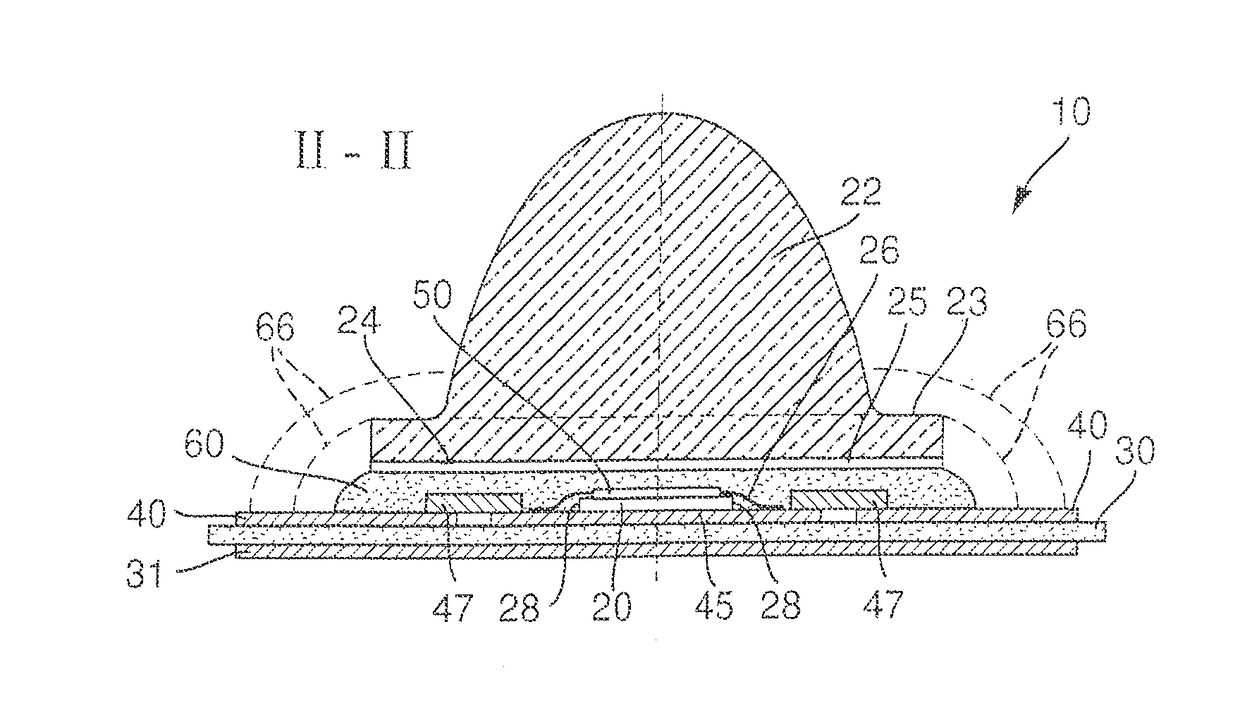
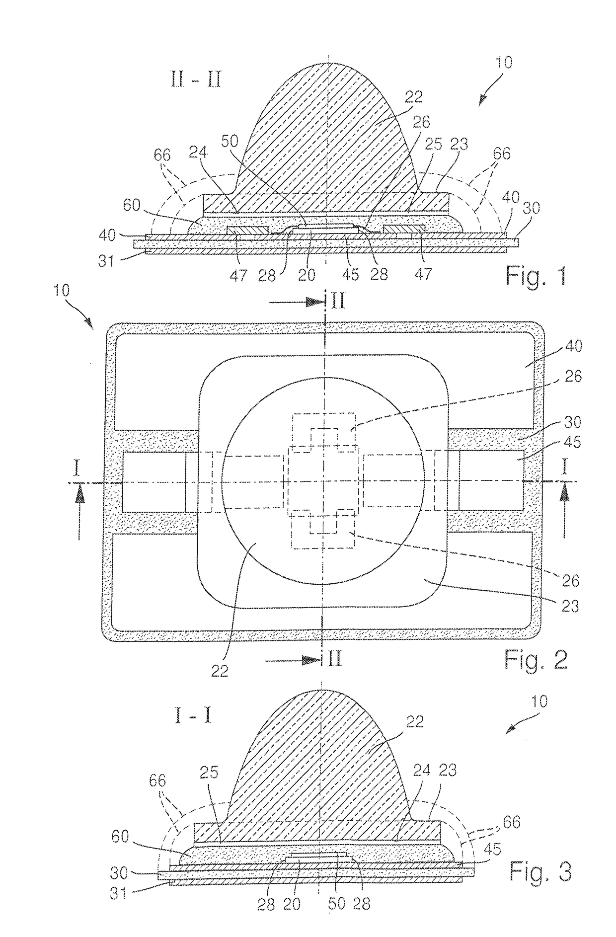
[0012]An advantage of the device of the invention is that the secondary optical element has a planar surface and as a result can be manufactured simply and cost-effectively. Since a polymer adhesive layer, which comprises a silicone compound, is formed between the bottom side of the secondary optical element and the top side of the substrate or the front side of the solar cell, a frictional connection can be produced in a simple and cost-effective manner without other connecting means. Between the front side of the solar cell and the bottom side of the secondary optical element the polymer adhesive layer can be formed with a small thickness, preferably less than 2 mm, most preferably less than 0.5 mm. Experiments have shown that the adhesion between the polymer adhesive layer and the planar bottom side of the secondary optical element increases substantially with the formation of a thin adhesion-promoting layer and the reliability can be improved hereby. It is preferred to make the adhesion-promoting layer transparent and very thin; preferably the thickness is less than 0.5 mm, most preferably less than 0.05 mm. It turned out that the polymer adhesive layer has sealing properties, and the top side of the substrate and the semiconductor body and particularly the side surfaces of the semiconductor body are reliably protected by the polymer adhesive layer from environmental influences. Further experiments have shown that an additional sealing layer, which surrounds in particular the outer edge of the cushion-shaped polymer adhesive layer, becomes unnecessary. In this way, the number of manufacturing steps for producing the solar cell unit can be reduced further. An advantage of the cushion-shaped formation of the polymer adhesive layer below the planar surface is that there is no restriction for a lateral expansion of the polymer adhesive layer. An expansion or shrinking of the polymer adhesive layer both perpendicular to the direction of the top side of the substrate and also perpendicular to the direction due to a change in temperature and / or a change in moisture is hereby easily possible. This reduces the probability of a delamination between the polymer adhesive layer and the substrate.
[0013]In an embodiment, a second adhesion-promoting layer can be formed between the polymer adhesive layer and the front side of the semiconductor body, and the second adhesion-promoting layer is connected by material bonding to the front side of the semiconductor body. The reliability can be improved further with the formation of the second adhesion-promoting layer. According to an alternative embodiment, the second adhesion-promoting layer is also formed on the top side of the substrate. In a further refinement, the first adhesion-promoting layer is connected by material bonding with the entire bottom side of the secondary optical element.
[0016]In an embodiment, the substrate at least in one direction, preferably in both directions can be formed within the top side plane of the substrate, has a greater lateral extension than the secondary optical element. Experiments have shown that as a result according to a refinement the polymer adhesive layer projects laterally over the surface on the bottom side of the secondary optical element and an especially strong frictional connection of the secondary optical element with the substrate can be achieved.
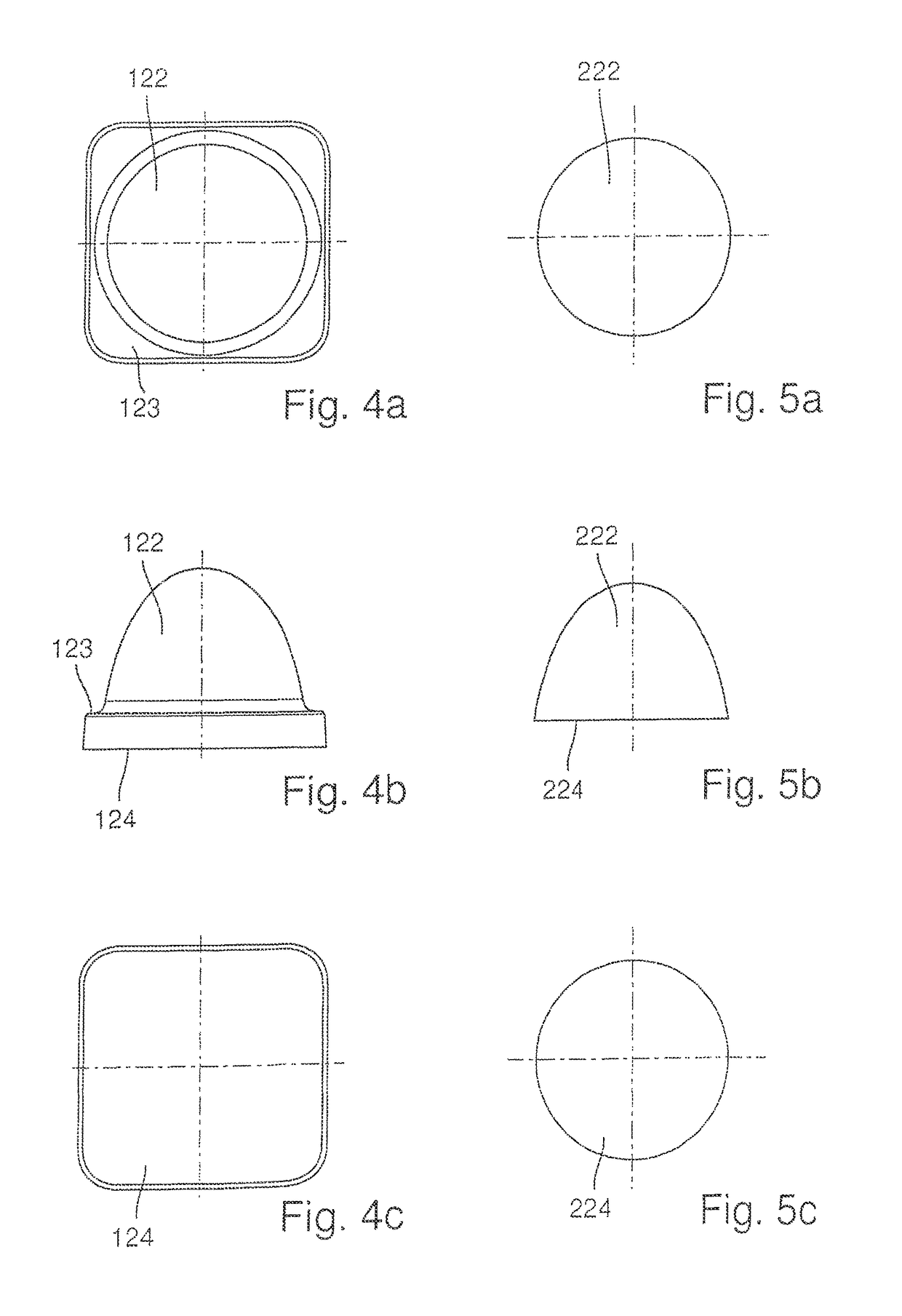
[0017]In an embodiment, the secondary optical element can be configured in the shape of a half-ellipsoid and preferably has a circumferential shoulder-shaped collar. In a further embodiment, the secondary optical element is configured in the shape of a truncated pyramid or funnel. It is preferred, furthermore, to make the secondary optical element as a single piece of an inorganic material, preferably of a quartz glass compound. An advantage of the inorganic material or quartz glass compound is the very good UV transparency and the extraordinary high temperature stability and high mechanical and chemical resistance in comparison with an organic or plastic compound.
[0018]In another embodiment, a metal layer can be formed on the bottom side of the substrate as part of the substrate, whereby the metal layer is preferably not formed in a circumferential edge region directly at the edge of the substrate. An advantage of the metal layer is that compared with a substrate without a back metal layer, the heat is transferred from the top side of the substrate uniformly to the entire substrate. Experiments have shown that a higher radiation from the bottom side also occurs due to the more uniform distribution of heat. Further, when the substrate is mounted on a base, the heat transfer resistance between the base and the substrate is reduced by means of the back metal layer.


