Compound, active light sensitive or radiation sensitive resin composition, resist film using same, resist-coated mask blank, photomask, pattern forming method, method for manufacturing electronic device, and electronic device

a technology of active light sensitive or radiation sensitive resin and resin composition, which is applied in the direction of photomechanical equipment, originals for photomechanical treatment, instruments, etc., to achieve excellent pattern shape, high resolution, and high resolving power

Active Publication Date: 2018-02-27
FUJIFILM CORP
View PDF35 Cites 6 Cited by
  • Summary
  • Abstract
  • Description
  • Claims
  • Application Information

AI Technical Summary

Benefits of technology

[0008]An object of the present invention is to provide a compound and an active light sensitive or radiation sensitive resin composition which are able to form ultrafine (for example, a line width of 50 nm or less) patterns in a state in which high resolution (for example, high resolving power), excellent pattern shape, and low line edge roughness (LER) are satisfied at the same time.
[0034]According to the present invention, it is possible to provide a compound and an active light sensitive or radiation sensitive resin composition which are able to form ultrafine (for example, a line width of 50 nm or less) patterns in a state in which high resolution (for example, high resolving power), excellent pattern shape, and low line edge roughness (LER) are satisfied at the same time.

Problems solved by technology

However, from the viewpoint of the overall performance as a resist, finding an appropriate combination of the resin, the photoacid generator, the basic compound, the additives, the solvent, and the like to be used is difficult, in particular, in consideration of the current demand for forming ultrafine (for example, a line width of 50 nm or less) patterns with high resolution (for example, high resolving power), excellent pattern shape, and low line edge roughness (LER), there is room for improvement in practice.

Method used


Image

  • Compound, active light sensitive or radiation sensitive resin composition, resist film using same, resist-coated mask blank, photomask, pattern forming method, method for manufacturing electronic device, and electronic device
  • Compound, active light sensitive or radiation sensitive resin composition, resist film using same, resist-coated mask blank, photomask, pattern forming method, method for manufacturing electronic device, and electronic device
  • Compound, active light sensitive or radiation sensitive resin composition, resist film using same, resist-coated mask blank, photomask, pattern forming method, method for manufacturing electronic device, and electronic device

Examples


examples

[0416]More detailed description will be given below of the present invention using Examples; however, the content of the present invention is not limited thereto.

[0417]

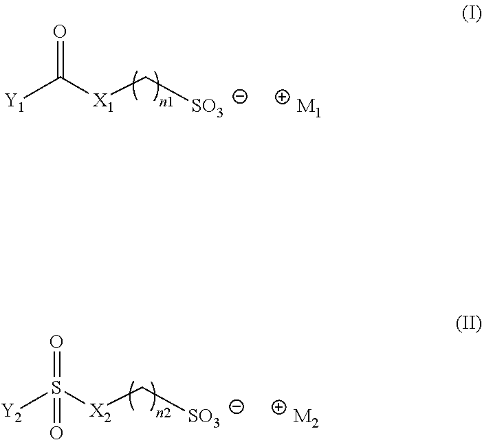
[0418]5.0 g of sodium 2-mercapto ethanesulfonate, 1.20 g of sodium hydroxide, 50 g of pure water, and 10 g of tetrahydrofuran (THF) were mixed and cooled to 0° C., then 6.05 g of adamantane carbonyl chloride was added thereto, and stirring was carried out for two hours at room temperature. Next, after adding a methanol solution of 10.45 g of triphenylsulfonium bromide and stirring for 30 minutes at room temperature, separation was carried out by adding pure water and ethyl acetate to the reaction mixture and the organic phase was cleaned with pure water, then the compound (A1) (12.3 g) was obtained by vacuum drying after distilling off the solvent under reduced pressure.

[0419]Here, the 1H-NMR spectrum of the compound (A1) (400 MHz, CDCl3) is δ=7.86-7.66 (m, 15H), 3.32-3.28 (m, 2H), 3.06-3.02 (m, 2H), and 2.06-1.64 (m,...

examples 1q to 11q

and Comparative Examples 1Q to 4Q

[0522](Preparation of Resist Solution)

[0523]A positive type resist solution was prepared by filtering the positive type resist composition shown in Table 4 above through a polytetrafluoroethylene filter having a pore size of 0.04 μm.

[0524](Resist Evaluation)

[0525]The prepared positive type resist solution was evenly coated on a silicon substrate subjected to a hexamethyldisilazane treatment using a spin coater, and a resist film having a film thickness of 50 nm was formed by heating and drying on a hot plate for 60 seconds at 100° C.

[0526]The sensitivity, the resolving power, the pattern shape, and the line edge roughness (LER) of the obtained resist film were evaluated using the following methods.

[0527][Sensitivity]

[0528]After performing exposure on the obtained resist film via a reflective-type mask with a 1:1 line and space pattern with a line width of 50 nm while changing the exposure amount by 0.1 mJ / cm2 at a time in a range of 0 mJ / cm2 to 20.0 ...

example 1e

[0540](2) Preparation of Resist Coating Solution

[0541](Coating Liquid Composition of Negative Type Resist Composition N1)

[0542]

Resin (P′-4)4.21 gCompound (A1) (photoacid generator, structural formula0.47 gdescribed above)Cross-linking agent CL-1 (structural formula described below)0.59 gCross-linking agent CL-4 (structural formula described below)0.30 gTetrabutyl ammonium hydroxide (basic compound)0.04 g2-hydroxy-3-naphthoic acid (organic carboxylic acid)0.11 gSurfactant PF6320 (produced by Omnova Solutions Inc.)0.005 g Propylene glycol monomethyl ether acetate (solvent)75.0 gPropylene glycol monomethyl ether (solvent)18.8 g

[0543]A resist coating solution was obtained by passing the composition solution described above through a microfilter with a polytetrafluoroethylene filter which has a pore size of 0.04 μm.

[0544](3) Creation of Resist Film

[0545]A resist film with a film thickness of 50 nm was obtained by coating the 6-inch wafers described above with a resist coating solution us...


PUM

PropertyMeasurementUnit
roughnessaaaaaaaaaa
thicknessaaaaaaaaaa
alkali dissolution speedaaaaaaaaaa

Abstract

Provided is an active light sensitive or radiation sensitive resin composition which contains a compound (A) represented by General Formula (I) or (II):in the formulae, each of Y1 and Y2 represents a monovalent organic group; each of M1+ and M2+ represents an organic onium ion; each of X1 and X2 represents a group that is represented by —S—, —NH—, or —NR1—; R1 represents a monovalent organic group; each of n1 and n2 represents an integer of 1 or more; and R1 and Y1 or Y2 may bond with each other to form a ring.

Description

CROSS REFERENCE TO RELATED APPLICATION[0001]This is a continuation of International Application No. PCT / JP2014 / 065498 filed on Jun. 11, 2014, and claims priority from Japanese Patent Application No. 2013-145015 filed on Jul. 10, 2013 and Japanese Patent Application No. 2014-026904 filed on Feb. 14, 2014, the entire disclosures of which are incorporated herein by reference.BACKGROUND OF THE INVENTION[0002]1. Field of the Invention[0003]The present invention relates to a compound, an active light sensitive or radiation sensitive resin composition, a resist film using the same, a resist-coated mask blank, a photomask, a pattern forming method, a method for manufacturing electronic device, and an electronic device, which are suitable for use in super-micro lithographic processes and other fabrication processes such as for manufacturing super LSIs or high capacity microchips and are capable of forming a high-definition pattern using electron beams or extreme ultraviolet light.[0004]2. De...

Claims


Application Information

Patent Timeline
Patent Type & Authority Patents(United States)
IPC IPC(8): G03F7/004H01L21/027C07D327/08C07C309/15C07D333/76C07C311/16C07C327/24C07C381/12C07D209/48C07D333/46C07D335/16C07D339/08C07C311/14C07D347/00C07C311/48C07C311/51C07C327/22C07C327/26C07D493/08C07C25/18C07J31/00C07J41/00C07C309/19C07C321/28C07C323/09C07C323/20H01L29/16G03F7/038G03F7/039
CPCG03F7/0045C07C25/18C07C309/15C07C309/19C07C311/14C07C311/16C07C311/48C07C311/51C07C321/28C07C323/09C07C323/20C07C327/22C07C327/24C07C327/26C07C381/12C07D209/48C07D327/08C07D333/46C07D333/76C07D335/16C07D339/08C07D347/00C07D493/08C07J31/006C07J41/0055C07J41/0061G03F7/0382G03F7/0392G03F7/0397H01L21/0271H01L21/0276H01L29/16C07C2601/08C07C2601/14C07C2602/42C07C2603/18C07C2603/24C07C2603/74G03F1/76G03F7/038
Inventor TSUCHIMURA, TOMOTAKA
Owner FUJIFILM CORP
Why Eureka
Try Eureka