Three-dimensional substrate for providing three-dimensional structure

a three-dimensional structure and substrate technology, applied in the direction of supporting structure mounting, casing/cabinet/drawer details, electrical equipment casings/cabinets/drawers, etc., can solve the problem that the multi-layer substrate cannot offer the three-dimensional structure having a different, cannot be three-dimensionally arranged, and the flexibility of home electronics or the like, etc. problem, to achieve the effect of easy stacked, easy enlargement, and convenient enlargemen

Active Publication Date: 2018-02-27
TAWARAYAMA MISAKO
View PDF19 Cites 0 Cited by
  • Summary
  • Abstract
  • Description
  • Claims
  • Application Information

AI Technical Summary

Benefits of technology

[0014]The inside of the electronic device is used as a circuit space and the electronic circuit itself is formed to be three-dimensional. Because of this, the electronic component can be connected vertically, laterally or obliquely in the electronic device. Thus, the capacity of the area for providing the electronic circuit can be enlarged. The electric component can be easily stacked on another electronic component and the wiring can be easily formed on the electronic component. Furthermore, the circuit is formed by being separated into a plurality of components. In addition, by mutually combining the components with each other so as to provide an electrical connection, the electronic devices having a complicated circuit and having an irregular shape such as a spherical shape can be provided. Since the substrate is not formed in a plate-like shape, the shape of the machine can be flexibly formed according to the demand of the design.

Problems solved by technology

Because of the plate-like shape, flexibility of the design of home electronics or the like is limited.
Thus, a linearly circuit cannot be formed on the upper part of the electronic components J. Furthermore, although the cord wiring can be arranged vertically, laterally or obliquely in a universal substrate, the cord cannot be three-dimensionally arranged since the components are fixed on a flat surface and therefore the cord is necessarily arranged along the surface.
The multilayer substrate cannot offer the three-dimensional structure having a different shape than the substrate.
Conventionally, the completed design of the electronic product is limited and the size of the electronic product becomes larger in many cases since the electronic circuits and other components are housed inside.

Method used


Image

  • Three-dimensional substrate for providing three-dimensional structure
  • Three-dimensional substrate for providing three-dimensional structure
  • Three-dimensional substrate for providing three-dimensional structure

Examples


Embodiment Construction

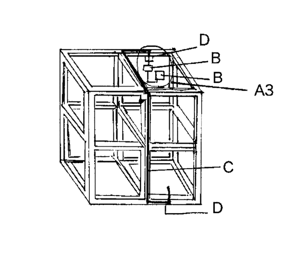
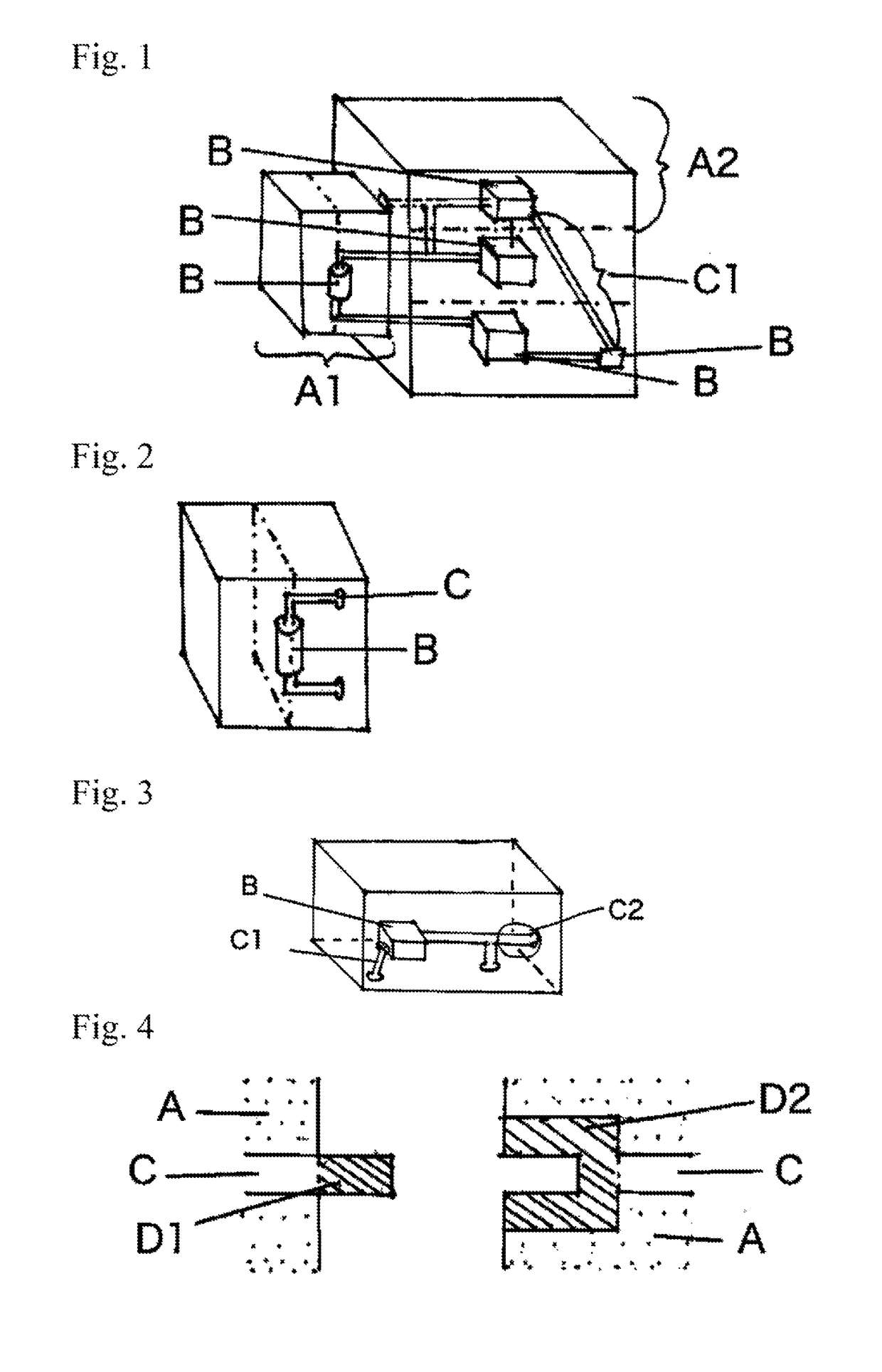
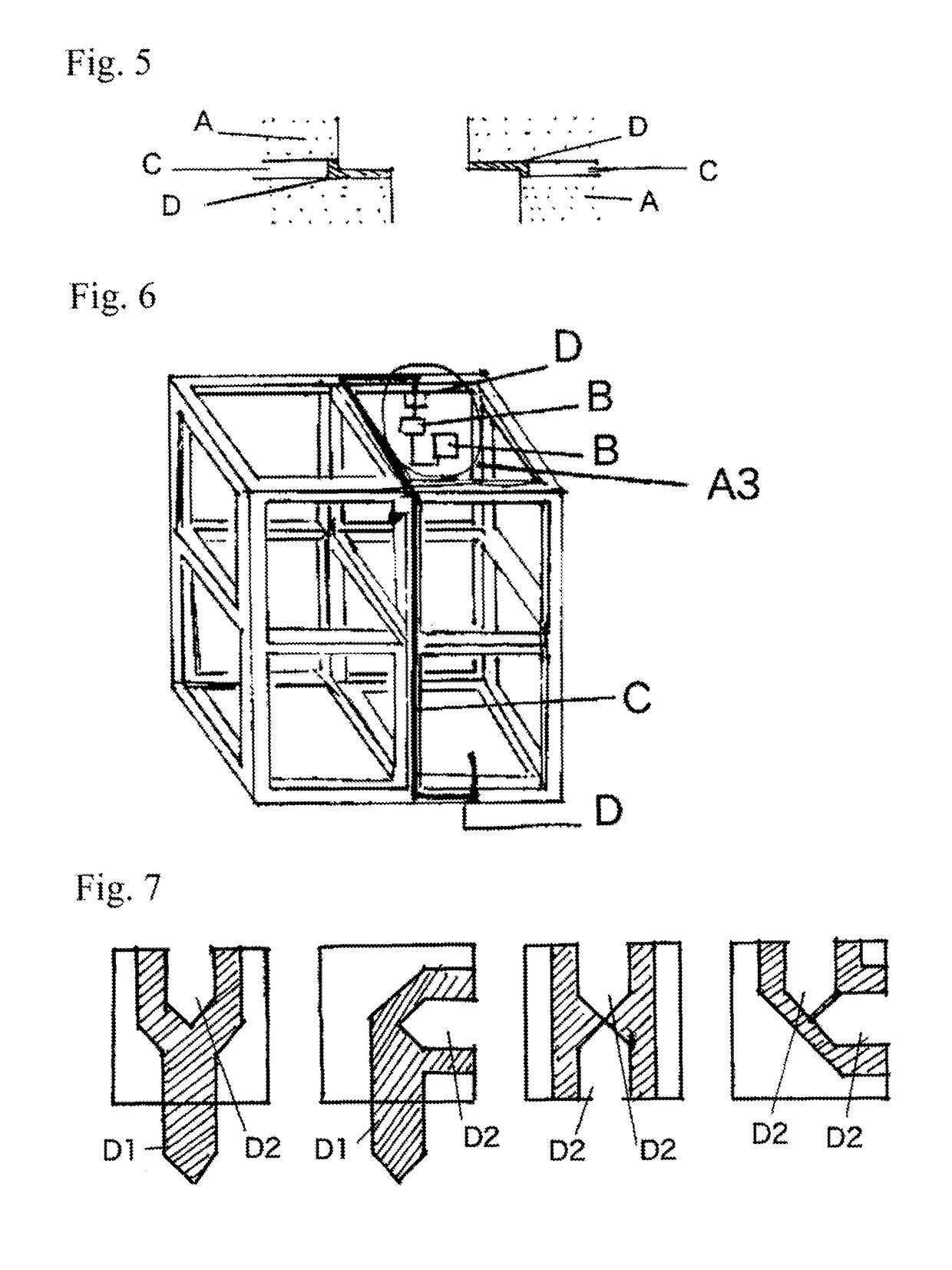
[0030]Hereafter, the present invention will be explained based on the embodiments. However, the present invention is not limited to the embodiments described below. In the explanation below, the three-dimensional substrate is formed so as to constitute a completed design when the assembling is finished. Namely, the three-dimensional substrate forms a three-dimensional structure by three-dimensionally constituting the cord. In addition, the three-dimensional substrate can be formed by combining a plurality of cords. Furthermore, a rigidity of the cord can be secured by forming the cord from an insulating material and a conductive material. The three-dimensional substrate is formed by using, for example, a computer graphics and considering a space as a substrate space. When the components are modeled by using the computer graphics, the components can be drawn by wire frames while the components are separated with a virtual line. The components drawn by the computer graphics are formed...


PUM


Abstract

The present invention provides a three-dimensional substrate having a different shape than the conventional circuit substrate when a plurality of components are combined to form an electronic circuit. In addition, an electronic device is provided from the three-dimensional substrate. The three-dimensional substrate forms a component forming the three-dimensional structure by three-dimensionally forming the electronic circuit. The component includes at least one electronic component and an electric connection structure for electrically connecting the electronic component with the outside the component. When a plurality of components are combined, the electronic device having the three-dimensional shape having a different shape than the component is formed. The present invention provides the three-dimensional substrate capable of being designed by the shape of the substrate itself.

Description

CROSS-REFERENCES TO RELATED APPLICATIONS[0001]This Application claims the benefit of priority and is a Continuation application of the prior International Patent Application No. PCT / JP2015 / 006317, with an international filing date of PCT / JP2015 / 006317, which designated the United States, and is related to the Japanese Patent Application No. 2015-010709, filed Jan. 5, 2015, the entire disclosures of all applications are expressly incorporated by reference in their entirety herein.BACKGROUND OF THE INVENTION[0002]1. Field of the Invention[0003]The present invention relates to a technology to make an electronic circuit substrate three-dimensional. More specifically, the present invention relates to a three-dimensional (solid) substrate and an electronic device formed by the three-dimensional substrate so that the three-dimensional structure having a different shape than the electronic circuit substrate is formed when a plurality of components are combined to form an electronic circuit....

Claims


Application Information

Patent Timeline
Patent Type & Authority Patents(United States)
IPC IPC(8): H05K7/02H05K5/02H05K7/14
CPCH05K7/023H05K7/14H05K5/0247H05K1/14H05K1/0284H05K1/0286H05K2201/09963
Inventor TAWARAYAMA, MISAKO
Owner TAWARAYAMA MISAKO
Why Eureka
Try Eureka