Light-emitting device package and light-emitting module including the same

a technology of light-emitting devices and light-emitting modules, which is applied in the direction of basic electric elements, semiconductor devices, electrical equipment, etc., can solve the problems of color deviation (or color separation), deterioration of light characteristics, and complicated manufacturing process

Active Publication Date: 2018-03-27
SUZHOU LEKIN SEMICON CO LTD
View PDF4 Cites 0 Cited by
  • Summary
  • Abstract
  • Description
  • Claims
  • Application Information

AI Technical Summary

Benefits of technology

[0010]Embodiments provide a light-emitting device package capable of preventing color deviation and a light-emitting module including the same.

Problems solved by technology

In a conventional light-emitting device package including LEDs, yellow light is emitted through the center of the upper surface thereof, whereas blue light is emitted through the corner between the upper surface and the side surface thereof, which may cause color deviation (or color separation).
When an anisotropic secondary lens is applied to solve this problem, the characteristics of the light may be deteriorated and the manufacturing process may be complicated due to design difficulties and inferior fabrication technologies.
In particular, in the case of a conventional integrated type light-emitting device package in which a lens and a light-emitting device are in contact with each other, rather than being spaced apart from each other, an anisotropic aspheric lens is necessary, which may result in design difficulties and more serious color deviation.

Method used


Image

  • Light-emitting device package and light-emitting module including the same
  • Light-emitting device package and light-emitting module including the same
  • Light-emitting device package and light-emitting module including the same

Examples


Embodiment Construction

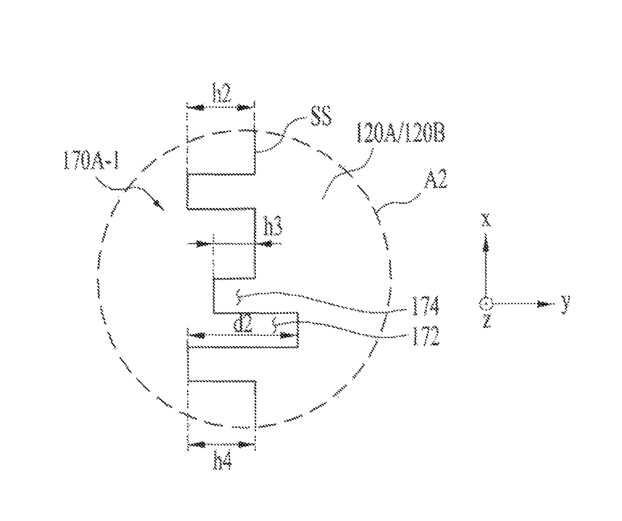
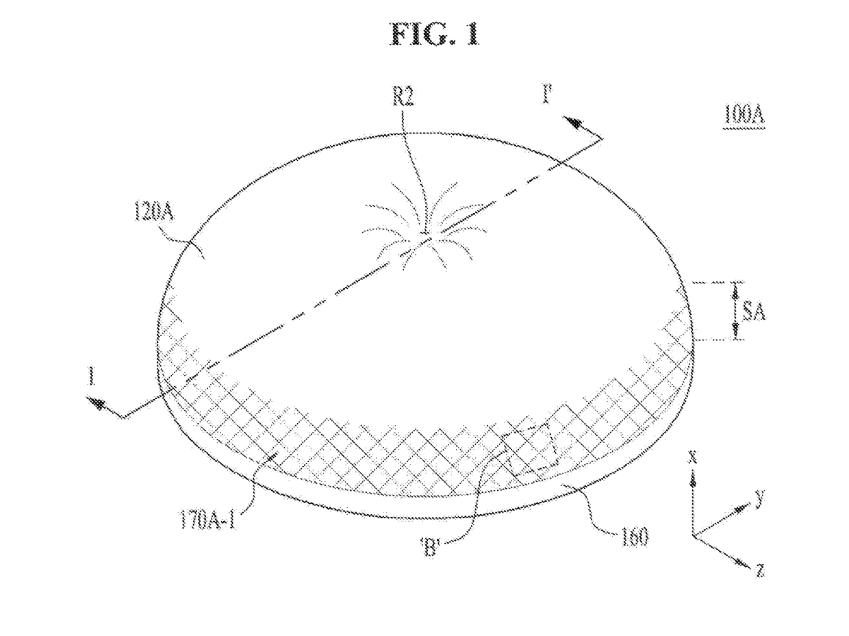
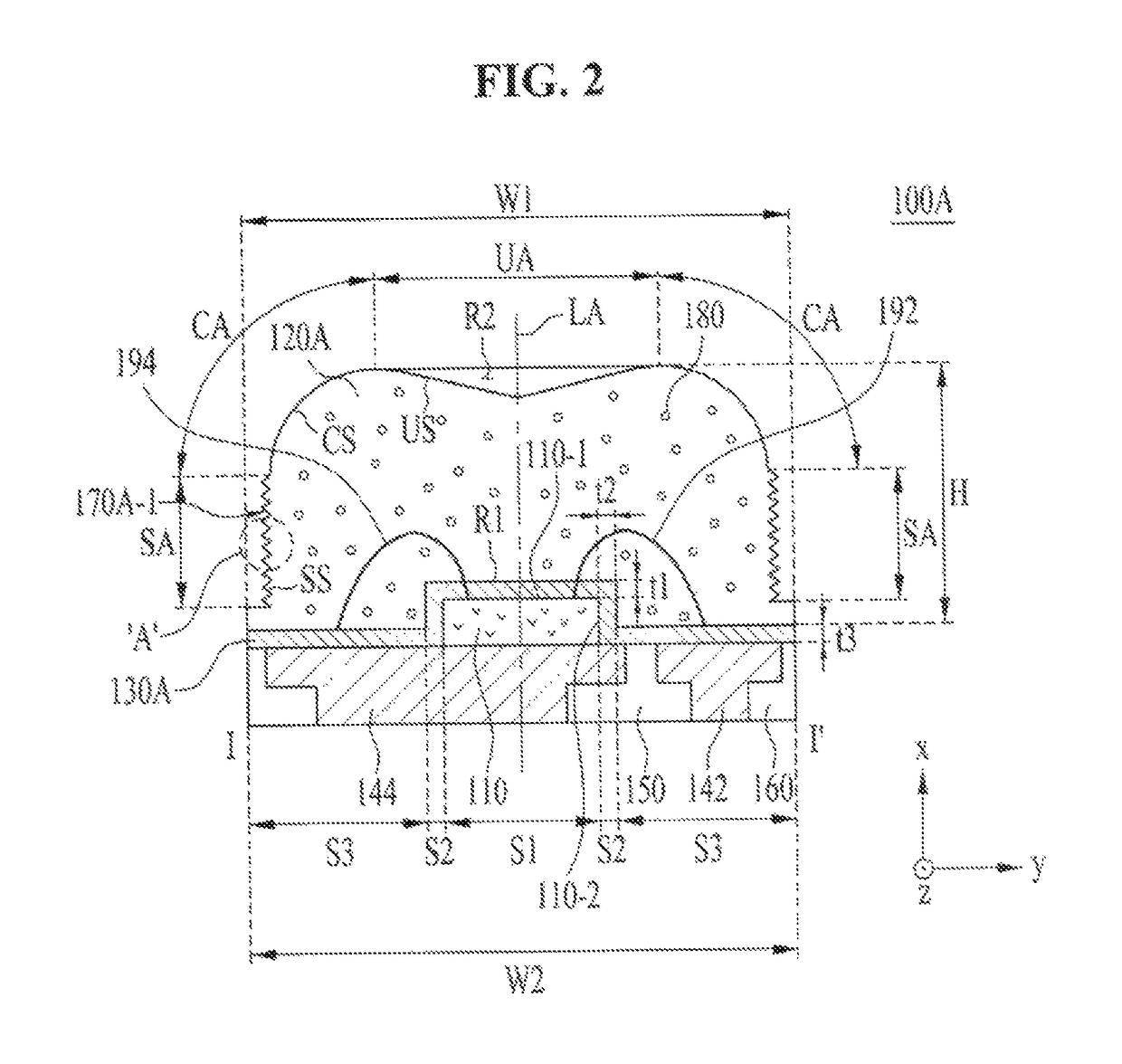
[0040]Hereinafter, exemplary embodiments will be described in detail with reference to the accompanying drawings to aid in understanding of the embodiments. However, the embodiments may be altered in various ways, and the scope of the embodiments should not be construed as limited to the following description. The embodiments are intended to provide those skilled in the art with more complete explanation.

[0041]In the following description of the embodiments, it will be understood that, when each element is referred to as being formed “on” or “under” the other element, it can be directly “on” or “under” the other element or be indirectly formed with one or more intervening elements therebetween. In addition, it will also be understood that “on” or “under” the element may mean an upward direction and a downward direction of the element.

[0042]In addition, the relative terms “first”, “second”, “upper”, “lower” and the like in the description and in the claims may be used to distinguish ...


PUM


Abstract

Embodiments provide a light-emitting device package including a light source, a lens disposed on the light source, and a diffuser located on at least one of the interior of the lens or a light emission surface of the lens, so as to diffuse light. The diffuser includes at least one of a light dispersing agent distributed in the interior of the lens, or at least one light diffusion structure located on at least one of the outside or the inside of the light emission surface of the lens. The light diffusion structure includes a rough surface formed on the light emission surface of the lens.

Description

CROSS REFERENCE TO RELATED APPLICATION[0001]This application claims priority under 35 U.S.C. §119 to Korean Patent Application No. 10-2014-0161531, filed on Nov. 19, 2014, which is hereby incorporated in its entirety by reference as if fully set forth herein.BACKGROUND OF THE INVENTION[0002]1. Field of the Invention[0003]Embodiments relate to a light-emitting device package and a light-emitting module including the same.[0004]2. Description of Related Art[0005]Semiconductor Light-Emitting Diodes (LEDs) are semiconductor devices that convert electricity into light such as infrared light using the characteristics of compound semiconductors so as to enable transmission / reception of signals, or that are used as a light source.[0006]Group III-V nitride semiconductors are in the spotlight as core materials of light emitting devices such as, for example, LEDs or Laser Diodes (LDs) due to physical and chemical characteristics thereof.[0007]The LEDs do not include environmentally harmful mat...

Claims


Application Information

Patent Timeline
Patent Type & Authority Patents(United States)
IPC IPC(8): H01L33/54H01L33/58H01L33/44H01L33/50H01L33/62
CPCH01L33/58H01L33/54H01L33/44H01L33/50H01L33/62H01L2224/48091H01L2933/0091H01L2224/8592H01L2933/0083H01L2924/00014
Inventor JOO, YANG HYUNLEE, CHANG HYUCKKANG, BO RAKIM, SUNG PHILSON, CHANG GYUN
Owner SUZHOU LEKIN SEMICON CO LTD
Why Eureka
Try Eureka