Supercharge Your Innovation With Domain-Expert AI Agents!

Impedance blocking filter circuit

a filter circuit and filter circuit technology, applied in the field of telecommunication systems, can solve the problems of significant limit or reduction of data rate, and achieve the effect of effectively and efficiently eliminating adsl interferen

Inactive Publication Date: 2010-03-16
PULSE ELECTRONICS
View PDF24 Cites 0 Cited by
  • Summary
  • Abstract
  • Description
  • Claims
  • Application Information

AI Technical Summary

Benefits of technology

"The present invention provides an impedance blocking filter circuit that effectively and efficiently eliminates ADSL interference caused by telephone terminal equipment. The circuit includes first, second, and third inductors connected in series between a first input terminal and a first common point. A first resistor has one end connected to the first common point and the other end connected to a first output terminal. A second inductor has one end connected to the second input terminal and the other end connected to a second common point. A second resistor has one end connected to the second input terminal and the other end connected to a second output terminal. A capacitor has one end connected to the first common point and the other end connected to the second common point. The circuit can be easily connected in series with the offending telephone terminal equipment. The filter circuit is modular in design and includes a plurality of components. The circuit effectively blocks impedance above 20 KHz to prevent interference from the customer's terminal equipment."

Problems solved by technology

However, since one or more telephone subscriber terminal equipment such as telephone sets, facsimile machines and / or answering devices are also connected to the same incoming telephone lines via internal house wiring, ADSL interference problems may be caused by the terminal equipment which can significantly limit or reduce the data rate.

Method used


Image

  • Impedance blocking filter circuit
  • Impedance blocking filter circuit
  • Impedance blocking filter circuit

Examples


Embodiment Construction

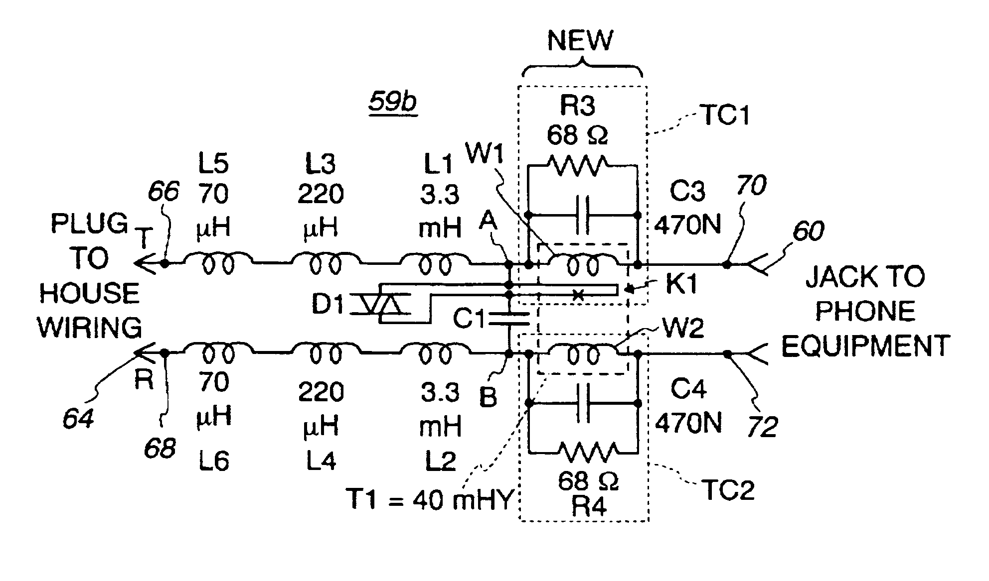
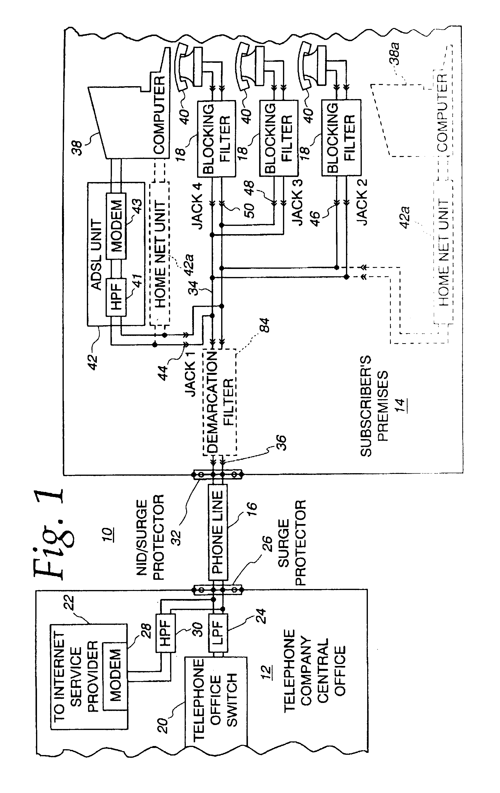
[0052]Referring now in detail to the drawings, there is illustrated in FIG. 1 an overall block diagram of a telecommunication system 10 for interconnecting a telephone company's central office (CO) 12 and a subscriber's premises 14 over a transmission media such as a conventional twisted pair of telephone lines 16. The telecommunication system 10 employs a plurality of impedance blocking filter circuits, constructed in accordance with the principles of the present invention, in which each is contained in a modular housing 18.

[0053]The central office 12 includes a telephone office switch 20 and an Internet Service Provider (ISP) 22. The telephone office switch 20 is used to send voice signals via a low-pass filter 24 and a surge protector 26 to the telephone line 16. The ISP 22 transmits ADSL data signals to a modem 28 which are then sent to the telephone lines 16 via a high-pass filter 30 and the surge protector 26. It should be understood that the voice signals from the telephone o...


PUM


Abstract

An impedance blocking filter circuit is provided for use in telecommunication systems for interconnecting between incoming telephone lines and customer's terminal equipment so as to unconditionally block impedances above 20 KHza desired frequency range due to the customer's terminal equipment from an ADSLa DSL network unit and / or home networking interface unit. The filter circuit includes first, second, and third inductors connected in series between a first input terminal and a first common point. A first resistor has its one end connected also to the first common point and its other end connected to a first output terminal. Fourth, fifth and sixth inductors are connected in series between a second input terminal and a second common point. A second resistor has its one end also connected to the second common point and its other end connected to a second output terminal. A capacitor has its ends connected across the first and second common points. In other aspects, the filter circuit also includes switching means for eliminating shunt additive capacitance, correction circuit means reducing significantly return loss, and switch suppression circuit means for eliminating transients.In one exemplary embodiment, the filter circuit is adapted to block impedances above 20 KHz and comprises a series of inductors disposed electrically between respective ones of first and second input terminals and output terminals. First and second switches responsive to loop current are disposed in series with respective capacitors between the series of inductors.

Description

CROSS-REFERENCE TO RELATED APPLICATIONS[0001]The present inventionapplication is a reissue of U.S. Pat. No. 6,212,259 issued Apr. 3, 2001 of the same title, which is a continuation-in-part application based on prior Ser. No. 09 / 370,137 filed on Aug. 9, 1999, <?insert-start id="INS-S-00005" date="20100316" ?>now U.S. Pat. No. 6,181,777, <?insert-end id="INS-S-00005" ?>which is, in turn, a continuation-in-part application based on parent application Ser. No. 09 / 195,522 filed on Nov. 19, 1998, <?delete-start id="DEL-S-00005" date="20100316" ?>and entitled “Impedance Blocking Filter Circuit.”<?delete-end id="DEL-S-00005" ?> <?insert-start id="INS-S-00006" date="20100316" ?>of the same title, now U.S. Pat. No. 6,188,750. This application is also related to co-pending reissue continuation application Ser. No. 10 / 748,729 filed Dec. 29, 2003 of the same title.<?insert-end id="INS-S-00006" ?>BACKGROUND OF THE INVENTION[0002]1. Field of the Invention[00...

Claims


Application Information

Patent Timeline
Patent Type & Authority Patents(United States)
IPC IPC(8): H04M1/24H04M1/00H04M11/00H04M9/00H03G7/00H04M1/738H03G11/00H03H1/00H03H7/01H03H7/06H03H7/09H03H9/46H04M1/74H04M3/00H04M11/06
CPCH03G7/00H03G11/00H03H7/06H03H2001/005H04M11/062H03H7/427H03H7/1783H03H7/0107H03H1/0007H03H7/0115H03H9/46
Inventor KIKO, FREDERICK J.
Owner PULSE ELECTRONICS
Features
  • R&D
  • Intellectual Property
  • Life Sciences
  • Materials
  • Tech Scout
  • Unparalleled Data Quality
  • Higher Quality Content
  • 60% Fewer Hallucinations
Learn More