Method for realizing SDRAM compatible design

A row address and column address technology, applied in the field of address multiplexing logic and SDRAM implementation compatibility, to achieve the effect of convenient logic implementation and simple operation

Inactive Publication Date: 2007-10-17
HUAWEI TECH CO LTD
View PDF4 Cites 0 Cited by
  • Summary
  • Abstract
  • Description
  • Claims
  • Application Information

AI Technical Summary

Problems solved by technology

[0011] The purpose of the present invention is to propose a method for realizing SDRAM compatible design, aiming at the problem that SDRAM with different capacity causes the linear address information of processor to change greatly, a solution is proposed, which does not require processor CPU and address multiplexing logic unit Handshake between, and the address multiplexing logic unit does not need to enumerate different address multiplexing methods in advance

Method used


Image

  • Method for realizing SDRAM compatible design
  • Method for realizing SDRAM compatible design
  • Method for realizing SDRAM compatible design

Examples


Embodiment Construction

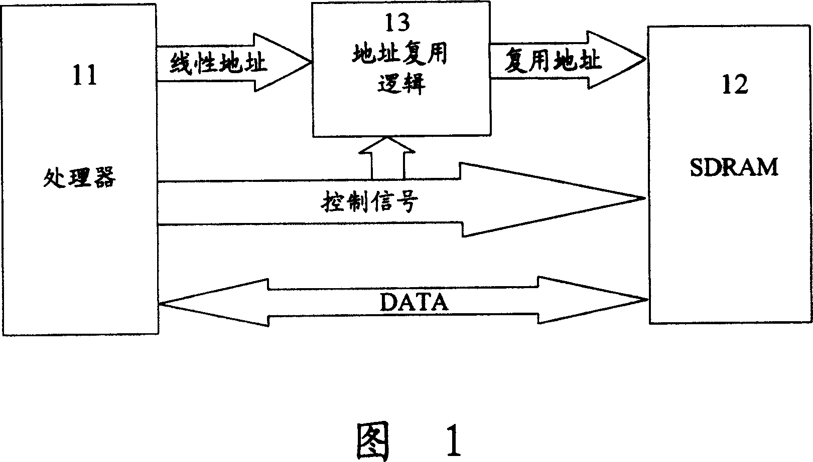
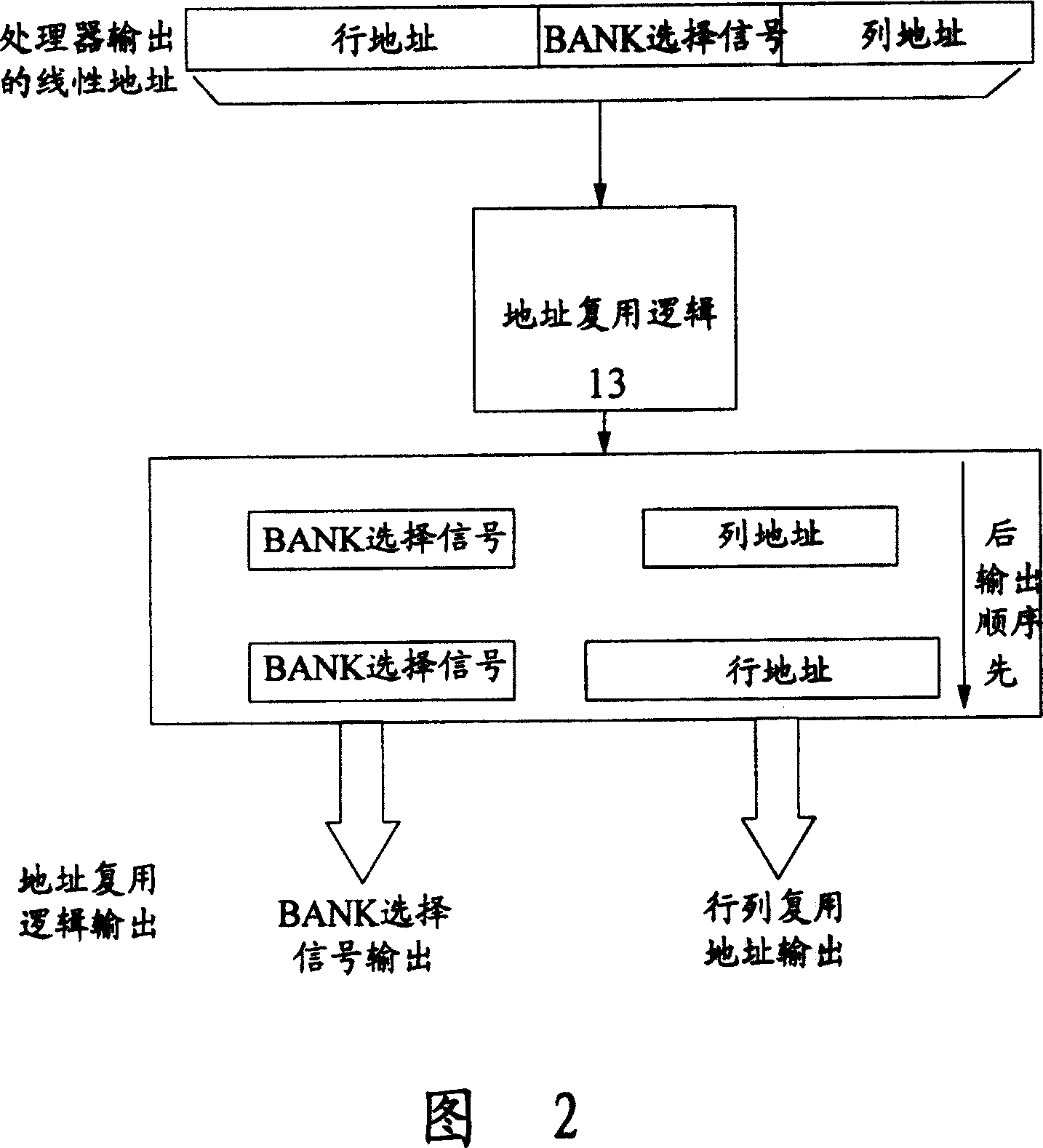
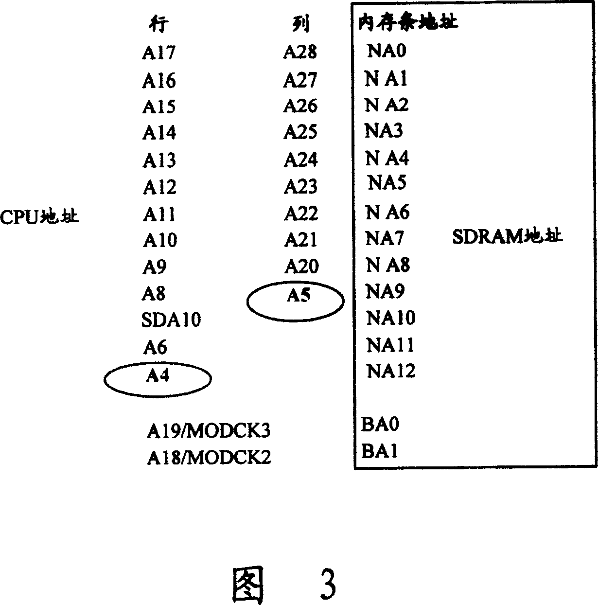
[0025] The technical scheme of the present invention realizes compatibility with SDRAM by adopting the method of row and column address conversion. In the case of an increase in the column address, the processor CPU can increase the row address, and the address multiplexing logic unit converts the row address into a column address, so as to be compatible with SDRAMs of different specifications.

[0026] At present, the development trend of SDRAM has undergone specification changes from 12 rows × 9 columns to 12 rows × 10 columns and then to 13 rows × 10 columns. It can be seen that the row and column addresses have an increasing trend. If it is just a simple increase of the row address, the compatible design of the address multiplexing logic unit can be realized more conveniently, but it is more difficult to realize the increase of the column address, because the increase of the column address will involve the position change of the row address and the bank selection signal. I...


PUM


Abstract

A method for realizing SDRAM compatible design includes keeping BANK selection address of processor CPU and pin position of column address unchanged, using a basic line and column disposed SDRAM as base to up-grade SDRAM, increasing line address only on addres high order pin position by processor CPU, driving SDRAM address line with different volume by address multiplexing logic unit through line-column conversion for carrying out compatibility for SDRAM with various volumes.

Description

technical field [0001] The present invention relates to an application technology of SDRAM, more precisely, it relates to the technology of realizing compatibility between address multiplexing logic and SDRAM, which can be applied to any occasion using processor and memory, such as communication, computer, artificial intelligence, instrumentation, etc. . Background technique [0002] In some cases, the address sent by the SDRAM controller of the processor is a linear address, but the address required by the SDRAM and the memory stick using the SDRAM is a row and column multiplexed address (such as multiplexing the memory stick address NA0- NA12 is the row address and column address), in order to allow the processor to access SDRAM, an address multiplexing logic unit must be added between the processor and SDRAM, and this address multiplexing logic unit performs row, Column multiplexing, and then send the multiplexed row and column addresses to SDRAM or SDRAM memory stick. T...

Claims


Application Information

Patent Timeline
Patent Type & Authority Patents(China)
IPC IPC(8): G06F12/00G06F12/10
Inventor 方卫峰魏孔刚李友谊牛从亮谢建湘
Owner HUAWEI TECH CO LTD
Why Eureka
Try Eureka