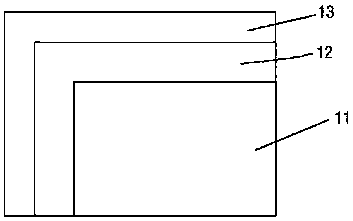
An outer pin pressing area of ​​a panel

A technology of press-fit area and outer pins, which is applied in the direction of instruments, nonlinear optics, optics, etc., can solve the problem of high cost, achieve the effects of improving yield, saving costs, and reducing the risk of misjudgment

Active Publication Date: 2019-10-25
TCL CHINA STAR OPTOELECTRONICS TECH CO LTD
View PDF10 Cites 0 Cited by
  • Summary
  • Abstract
  • Description
  • Claims
  • Application Information

AI Technical Summary

Problems solved by technology

[0004] like figure 2 As shown, the left side is the status of the panel before the Cell cutting process. Different products are completely the same at this stage, including the display area 11, the first TFT cutting line 131, the CF first cutting line 121, and the TFT second cutting line. Line 132, CF second cutting line 122, during Cell cutting process, cut along the different cutting lines designed in advance, just can obtain the product of two kinds of different frames, i.e. conventional frame panel (refer to figure 2 top right) and narrow bezel panels (reference figure 2 Bottom right), in the traditional design, two sets of masks are required for products with two different borders. Take the 4Mask TFT substrate as an example, when the border of the panel is changed, four masks need to be modified at the same time, resulting in higher product cost high

Method used


Image

  • An outer pin pressing area of ​​a panel
  • An outer pin pressing area of ​​a panel
  • An outer pin pressing area of ​​a panel

Examples


Embodiment approach 1

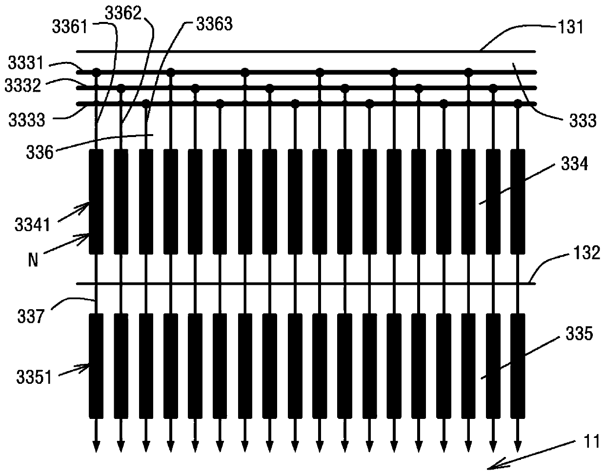
[0035] Such as image 3 It is a schematic diagram of the layout of the OLB area in the first embodiment of the present invention, including the first TFT cutting line 131, the first short wiring combination 333, the first group of bonding terminals 334, the second TFT cutting line 132, and the second group of bonding terminals 335. Display area 11.

[0036] combine image 3 To further illustrate, from the first TFT cutting line 131 to the display area 11, the first shorting wire combination 333, the first group of bonding terminals 334, the TFT second cutting line 132, the second Group bonding terminals 335 .

[0037] combine image 3 To further illustrate, the first short-circuit combination 333 and the first group of bonding terminals 334 are connected through a first metal wire 336, and the first group of bonding terminals 334 and the second group of bonding terminals 335 are connected through The second metal traces 337 are connected.

[0038] combine image 3 To fur...

Embodiment approach 2

[0045] Such as Figure 5 It is a schematic diagram of the layout of the OLB area in the second embodiment of the present invention, from Figure 5 It can be seen that in the second solution, a connecting unit 501 is added between the second TFT cutting line 132 and the second group of bonding terminals 335, and the connecting unit 501 is arranged on the second metal wiring 337 and disconnect the second metal trace 337 into two sub-segments 3371 and 3372 , and each of the second metal traces 337 is provided with one connection unit 501 .

[0046] combine Figure 5 To further illustrate, each of the connecting units 501 is staggered on the three adjacent second metal traces 337 and does not overlap each other. 6. 1+9... the connecting units are arranged on the same straight line, the 2nd, 2+3, 2+6, 2+9... the connecting units are arranged on the same straight line, the 3rd, 3+ 3, 3+6, 3+9... The connecting units are arranged on the same straight line.

[0047] combine Figu...


PUM


Abstract

The invention discloses an outer pin pressing zone of a face plate. The outer pin pressing zone comprises a TFT first cutting line, a first shorting stub assembly, a first group of binding terminals, a TFT second cutting line, a second group of binding terminals and a display zone, wherein the first shorting stub assembly, the first group of binding terminals, the TFT second cutting line, the second group of binding terminals and the display zone are sequentially arranged starting from the TFT first cutting line from outside to inside, the first shorting stub assembly and the first group of binding terminals are connected through a first metal wire, the first group of binding terminals and the second group of binding terminals are connected through a second metal wire, and meanwhile a connecting unit is added between the TFT second cutting line and the second group of binding terminals. By the adoption of the outer pin pressing zone, a conventional-frame face plate and a narrow-frame face plate can be tested by adopting a conventional Cell lighting-on mode, and accordingly the face plate manufacturing cost is reduced.

Description

technical field [0001] The present invention relates to the technical field of thin film transistor liquid crystal display (TFT-LCD), in particular to an Out Lead Bonding (OLB) area of ​​a panel. Background technique [0002] In the market, LCD panels all have a bezel. According to the width of the bezel, the panels are divided into narrow bezel panels and regular bezel panels. Narrow bezel panels are a very important trend in current panel design, but regular bezel panels still occupy In a certain market, panels with different frame specifications will coexist in the market for a foreseeable period of time. [0003] figure 1 It is a schematic diagram of the panel frame, which can be a TFT-LCD panel or an OLED panel. Take the TFT-LCD panel as an example, such as figure 1 , the entire panel includes two substrates, namely a TFT substrate 13 and a CF substrate 12, with a display area 11 in the middle. When the panel is working normally, the display area 11 is responsible for...

Claims


Application Information

Patent Timeline
Patent Type & Authority Patents(China)
IPC IPC(8): G02F1/1345G02F1/1362
CPCG02F1/1345G02F1/136227
Inventor 杜鹏
Owner TCL CHINA STAR OPTOELECTRONICS TECH CO LTD
Why Eureka
Try Eureka