Method for generating solid memory address configuration

A technology of address configuration and memory lines, applied in static memory, memory address/allocation/relocation, read-only memory, etc., can solve problems such as large physical size, low storage capacity, and poor strength

Inactive Publication Date: 2008-04-09
SAMSUNG ELECTRONICS CO LTD
View PDF4 Cites 0 Cited by
  • Summary
  • Abstract
  • Description
  • Claims
  • Application Information

AI Technical Summary

Problems solved by technology

However, each of these memory types has one or more of the following limitations: large physical size, low storage capacity, relatively high cost, poor strength, slow access time, and high power consumption

Method used


Image

  • Method for generating solid memory address configuration
  • Method for generating solid memory address configuration
  • Method for generating solid memory address configuration

Examples


Embodiment Construction

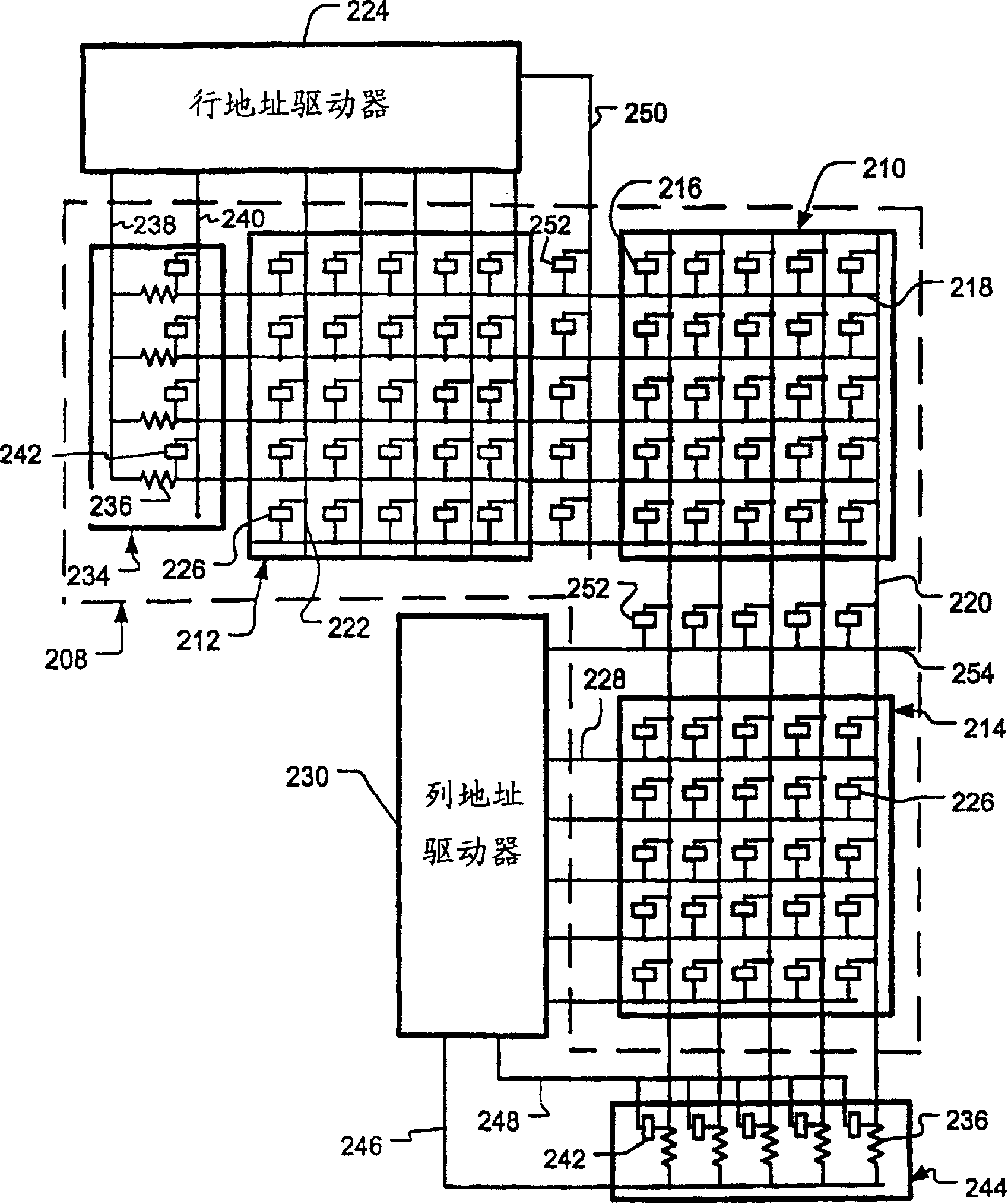
[0021] As shown in the drawings for illustrative purposes, the present invention is implemented in a diode-based OTP memory device. In the following paragraphs, the structure of the OTP storage device will be described, followed by the description of the two address protocols. An address protocol can provide fault-tolerant address configuration. Another address protocol may provide neighborhood disjoint address configuration as well as fault tolerant address configuration. Fault-tolerant address logic can improve manufacturing yields, and neighborhood-disjoint address logic allows memory devices to be formed at high resolution. Following the description of the address protocol is a description of a method of using look-up tables to extend address configuration to large storage arrays.

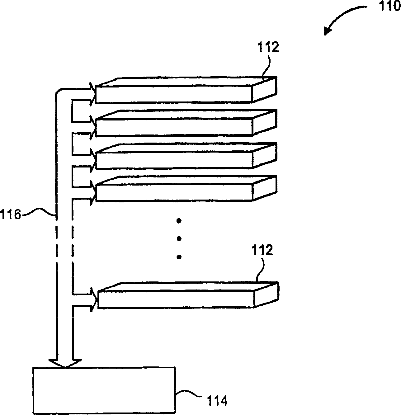
[0022] figure 1 A multi-layer solid state storage device 110 is shown. Multiple layers 112 are stacked on top of each other. Each layer 112 includes main memory and address logic. Layer 1...


PUM


Abstract

A method involves the use of a sequence of address configurations covering L memory lines and n address lines. The method includes forming L blocks (910). A most significant column of each block is filled with the sequence such that the most significant column of each block contains the same unshifted sequence (912). A least significant column of each block is filled with the sequence such entries in the least significant column of the blocks are shifted cyclically (914). The L blocks contain address configurations for L<2> memory lines and 2n address lines.

Description

technical field [0001] The present invention relates to information storage devices. More specifically, the present invention relates to address logic for solid-state memory. Background technique [0002] Portable devices such as PDAs, handheld computers, digital cameras, and digital music players include memory for storing data, digital images, and MP3 files. There are different types of memory available for these portable devices. Conventional memory types include flash memory, compact hard drives, compact disks, and magnetic tape. However, each of these memory types has one or more of the following limitations: large physical size, low storage capacity, relatively high cost, poor strength, slow access time, and high power consumption. [0003] A solid state diode based OTP memory is disclosed in assignee's US Serial No. 09 / 875,356 filed June 5, 2001. Compared with conventional memory, diode-based memory has high shock tolerance, low power consumption, fast access time...

Claims


Application Information

Patent Timeline
IPC IPC(8): G11C8/10G11C11/36G11C17/06G06F12/02G11C8/12
CPCG11C8/10G11C8/12G06F12/02
Inventor J·N·霍甘R·M·罗斯
Owner SAMSUNG ELECTRONICS CO LTD
Why Eureka
Try Eureka