Light emitting device and lighting device
一种发光装置、发光元件的技术,应用在照明装置、照明和加热设备、发光元件的半导体器件等方向,能够解决难以提高发光装置放射光强度和亮度、反射光强度衰减等问题,达到提高放射光强度及亮度、发光效率高的效果
- Summary
- Abstract
- Description
- Claims
- Application Information
AI Technical Summary
Problems solved by technology
Method used
Image
Examples
Embodiment 1
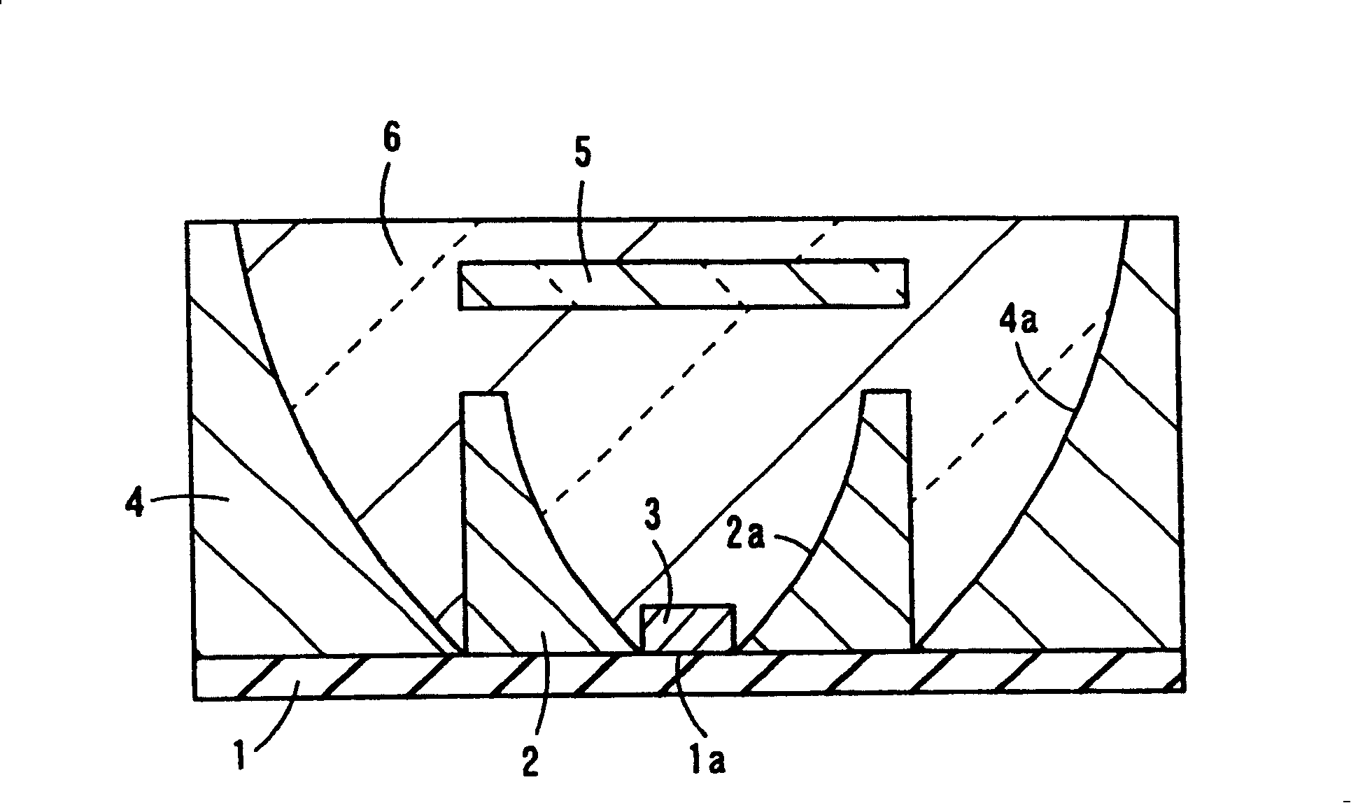
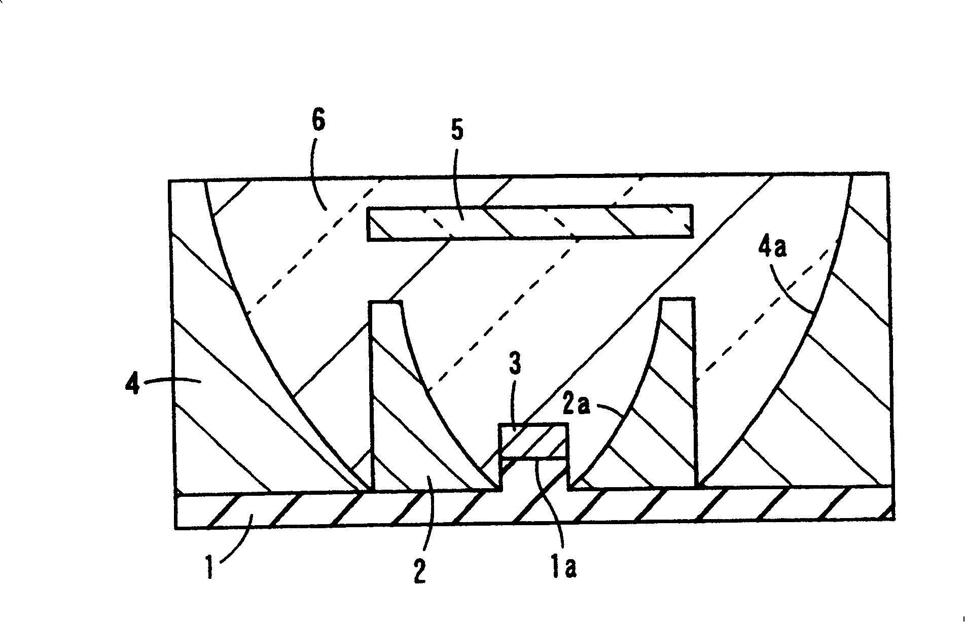
[0165] For the light-emitting device of the present invention, examples will be shown below. First, a base 1 made of alumina ceramics to be the base 1 was prepared. Moreover, substrate 1 such as image 3 As shown, it is integrally formed so that the placement portion 1a protrudes, and the upper surface of the placement portion 1a is parallel to the upper surface of the base body 1 other than the placement portion 1a.
[0166] The base 1 is a member in which a cuboid mounting part 1a of width 0.35 mm x depth 0.35 mm x thickness 0.15 mm is formed on the upper central part of a cuboid of width 17 mm x depth 17 mm x thickness 0.5 mm.
[0167] In addition, a wiring conductor for electrically connecting the light emitting element 3 and the external circuit board via internal wiring formed inside the base body 1 is formed at the portion where the light emitting element 3 is mounted on the placement portion 1a. The wiring conductor is made of a metallization layer made of Mo-Mn powd...
Embodiment 2
[0187] For the light-emitting device of the present invention, examples will be shown below. First, a substrate 1 made of alumina ceramics to be a substrate 1 was prepared. Moreover, substrate 1 such as Figure 16 As shown, it is integrally formed so that the placement portion 1a protrudes, and the upper surface of the placement portion 1a is parallel to the upper surface of the base body 1 other than the placement portion 1a.
[0188] The base 1 is a member in which a cuboid mounting part 1a of width 0.35 mm x depth 0.35 mm x thickness 0.15 mm is formed on the upper central part of a cuboid of width 17 mm x depth 17 mm x thickness 0.5 mm.
[0189] In addition, a wiring conductor for electrically connecting the light emitting element 3 and the external circuit board via internal wiring formed inside the base body 1 is formed at the portion where the light emitting element 3 is mounted on the placement portion 1a. The wiring conductor is made of a metallization layer made of ...
PUM
 Abstract
Description
Claims
Application Information


