High-voltage LED chip structure and manufacturing method thereof

A technology of LED chip and manufacturing method, which is applied in the direction of electrical components, electric solid devices, circuits, etc., can solve the problems of low output efficiency of high-voltage LED chips, and achieve the effect of providing luminous efficiency

Inactive Publication Date: 2019-05-28
XIAMEN CHANGELIGHT CO LTD
View PDF10 Cites 5 Cited by
  • Summary
  • Abstract
  • Description
  • Claims
  • Application Information

AI Technical Summary

Problems solved by technology

[0006] In view of this, the present invention provides a high-voltage LED chip structure and its manufacturing method to solve the problem that the output efficiency of high-voltage LED chips in the prior art is low and needs to be improved

Method used


Image

  • High-voltage LED chip structure and manufacturing method thereof
  • High-voltage LED chip structure and manufacturing method thereof
  • High-voltage LED chip structure and manufacturing method thereof

Examples


Embodiment Construction

[0044] As mentioned in the background art section, the output efficiency of the high-voltage LED chips in the prior art is relatively low and needs to be improved.

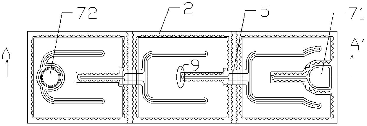
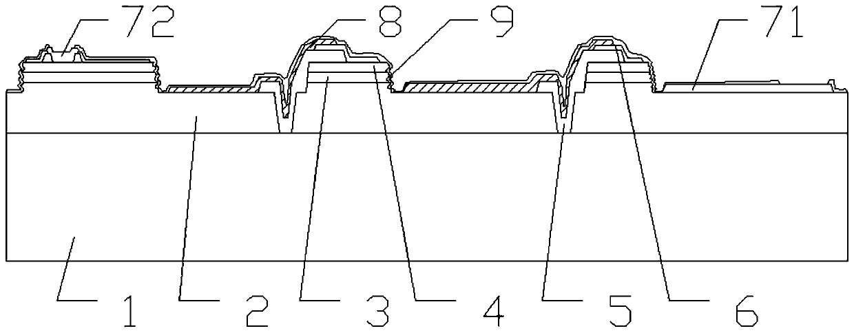
[0045] The inventor found that the reason for the above phenomenon is that the side wall of the high-voltage LED chip is a smooth plane. When the active layer emits light, there will be light emitted from the side. Since the high-voltage LED chip includes multiple adjacent LED sub-chips , if the light emitted from the side cannot be effectively utilized, the high-voltage LED chip will cause a large loss of light efficiency, resulting in a lower luminous output efficiency of the entire high-voltage LED chip compared to a single LED chip.

[0046] Based on this, the present invention provides a high-voltage LED chip structure, including:

[0047] Multiple LED sub-chips;

[0048] Each of the LED sub-chips includes:

[0049] Substrate;

[0050] an epitaxial layer located on the substrate, the epitaxial layer compri...


PUM


Abstract

The invention relates to a high-voltage LED chip structure and a manufacturing method thereof. The high-voltage LED chip structure comprises a plurality of LED sub-chips. wherein each LED sub-chip comprises a substrate, an epitaxial layer located on the substrate, a first electrode and a second electrode, the first electrode and the second electrode are located on the epitaxial layer, an isolationdeep groove is formed between every two adjacent LED sub-chips, and a bridging insulation isolation layer is arranged in a partial area of each isolation deep groove. And the side wall of the epitaxial layer corresponding to the part of the isolation deep grooves covered with the bridging insulation isolation layers is a non-coarsened side wall, and the side walls of the epitaxial layers in otherareas are coarsened side walls. The side wall of the epitaxial layer is coarsened, so that light which is directly emitted in the side direction can be reduced, the light which is emitted in the sidedirection is reflected to the front surface of the LED chip to be emitted, and the light emitting efficiency of the high-voltage LED chip structure is further improved. Meanwhile, the bridging insulation isolation layer is arranged to be a non-coarsened side wall, so that the problem of poor coverage of the insulation layer at the bridging position caused by coarsening of the side wall of the epitaxial layer can be avoided.

Description

technical field [0001] The invention relates to the technical field of manufacturing semiconductor devices, in particular to a high-voltage LED chip structure and a manufacturing method thereof. Background technique [0002] The light-emitting principle of light-emitting diodes (LEDs) is to use the energy difference between electrons moving between n-type semiconductors and p-type semiconductors to release energy in the form of light. This light-emitting principle is different from that of incandescent lamps, so light-emitting diodes are used called a cold light source. In addition, light-emitting diodes have the advantages of high durability, long life, light weight, and low power consumption. Therefore, today's lighting market places high hopes on light-emitting diodes and regards them as a new generation of lighting tools. [0003] However, the current LED chip still has the problem of low luminous efficiency. Therefore, improving the luminous efficiency of light-emitti...

Claims


Application Information

Patent Timeline
Patent Type & Authority Applications(China)
IPC IPC(8): H01L33/22H01L33/00H01L27/15
Inventor 刘英策李俊贤刘兆魏振东黄瑄
Owner XIAMEN CHANGELIGHT CO LTD
Why Eureka
Try Eureka