Organic light emitting display and method of fabricating the same

A light-emitting display, display technology, applied in the direction of organic semiconductor devices, semiconductor/solid-state device manufacturing, electroluminescence light source, etc., can solve problems such as short circuit

Active Publication Date: 2008-10-15
SAMSUNG DISPLAY CO LTD
View PDF4 Cites 0 Cited by
  • Summary
  • Abstract
  • Description
  • Claims
  • Application Information

AI Technical Summary

Problems solved by technology

As a result, when the opposite electrode 165 is formed on the pixel definition layer 155, a short circuit between the opposite electrode 165 and the pixel electrode 150 will occur.

Method used


Image

  • Organic light emitting display and method of fabricating the same
  • Organic light emitting display and method of fabricating the same
  • Organic light emitting display and method of fabricating the same

Examples


Embodiment Construction

[0015] The present invention will now be described more fully with reference to the accompanying drawings, in which exemplary embodiments are shown. Embodiments may take various forms and should not be construed as limited to the specific embodiments set forth herein. The thickness of regions or layers shown in the figures are exaggerated for clarity. Throughout the specification, the same reference numerals are used to denote the same elements.

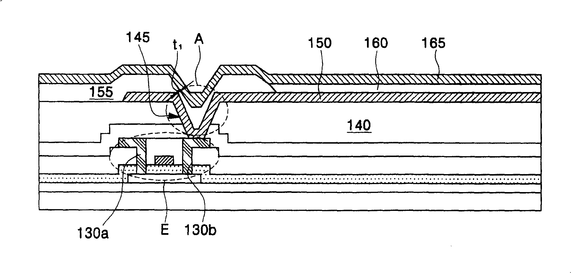
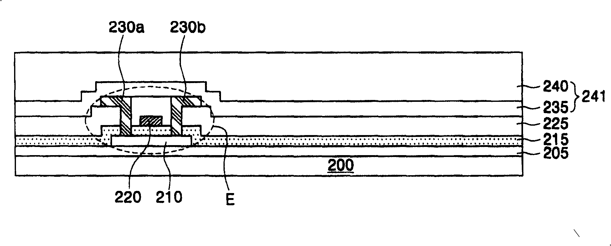
[0016] Figure 3C is a cross-sectional view of a unit pixel of the organic light emitting display (OLED) according to the first exemplary embodiment. refer to Figure 3C , a thin film transistor (TFT) “E” including a semiconductor layer 210 , a gate electrode 220 , a source electrode 230 a and a drain electrode 230 b is disposed on the substrate 200 . An insulating layer (not shown) is provided on the TFT "E". The insulating layer may include one or more inorganic layers, and / or one or more organic layers.

[0017] For example,...


PUM


Abstract

In one embodiment, an organic light emitting display (OLED) includes a thin film transistor (TFT) disposed on a substrate. In additiona, the display includes: an insulating layer disposed on the TFT and having a via hole; a pixel electrode disposed on the insulating layer and connected to a drain electrode of the TFT through the via hole; an emission layer disposed on the pixel electrode; and an opposite electrode pattern disposed on the emission layer and exposing at least an upper region of the via hole. This avoids close configuration proximity between the opposite electrode and the pixel layer thus reducing the possibility of a short circuit.

Description

technical field [0001] The present invention relates to an organic light emitting display (OLED) and a manufacturing method thereof, and more particularly, to an OLED and a manufacturing method thereof capable of substantially preventing a short circuit between a pixel electrode and a counter electrode. Background technique [0002] Organic Light Emitting Displays (OLEDs) are very suitable for displaying moving images regardless of their size, because OLEDs have a fast response speed of 1 ms or less, low power consumption, and are emissive display elements, so they have wide viewing angle. In addition, OLEDs can be manufactured at low temperatures and in simple processes based on conventional semiconductor manufacturing techniques. For these reasons, OLEDs have attracted much attention as next-generation flat panel display (FPD) elements. [0003] figure 1 is a cross-sectional view of a unit pixel of a conventional OLED. [0004] refer to figure 1 , the pixel electrode ...

Claims


Application Information

Patent Timeline
Patent Type & Authority Patents(China)
IPC IPC(8): H01L27/32H01L21/82H05B33/12H05B33/10
CPCH01L2251/558H01L51/0023H01L27/3244H01L51/0021H01L51/5206H01L51/5221H01L27/3246H10K59/122H10K59/12H10K71/621H10K71/60H10K50/81H10K50/822H10K50/82H10K2102/341H10K2102/351H05B33/26H05B33/10
Inventor 姜泰旭金茂显
Owner SAMSUNG DISPLAY CO LTD
Why Eureka
Try Eureka