Uncut chip substrate

A technology for cutting chips and substrates, used in lighting and heating equipment, light source fixing, electric solid devices, etc., can solve problems such as reduced productivity, degradation of heat dissipation characteristics, burr generation, etc., to achieve uniform heat dissipation characteristics, improve heat dissipation performance, and reduce the possibility of sexual effect

Inactive Publication Date: 2018-07-20
POINT ENG
View PDF3 Cites 0 Cited by
  • Summary
  • Abstract
  • Description
  • Claims
  • Application Information

AI Technical Summary

Problems solved by technology

[0011] However, according to the above-mentioned optical device of the prior art, since there is a limit in reducing the thickness of the adhesive TIM layer 10, even if a material having a good heat transfer rate is used, there is a problem of degrading heat dissipation characteristics due to its thickness.
Moreover, the productivity is reduced due to the manual process of precisely aligning the optics on the heat sink, and there is no guarantee of uniformity due to differences in the overall deposition thickness of the adhesive TIM layer or local thickness differences depending on the quality of work by the workers. The problem of heat dissipation characteristics of the
[0012] In addition, since the process of forming an electrical insulating layer via anodizing the upper surface of the heat sink 20 requires electrical insulation, there is a problem of increasing the above-mentioned process.
[0013] Most importantly, for existing technologies such as Figure 1a Each individual unit optical device fabricated from the base substrate (A) shown for the optical device, for example, for Figure 1a The rightmost separation of optical devices, such as figure 2 Burrs are shown at the far left during a separation process such as cutting or cutting, which can damage the very thin layer of anodized insulating layer 22 formed on the upper surface of heat sink 20 due to the gap between substrate 30 and heat sink 20. Insulation breakdown between the

Method used


Image

  • Uncut chip substrate
  • Uncut chip substrate
  • Uncut chip substrate

Examples


Embodiment Construction

[0045] Hereinafter, preferred exemplary embodiments of a method of manufacturing an optical device, and an optical device manufactured thereby will be described in detail with reference to the accompanying drawings.

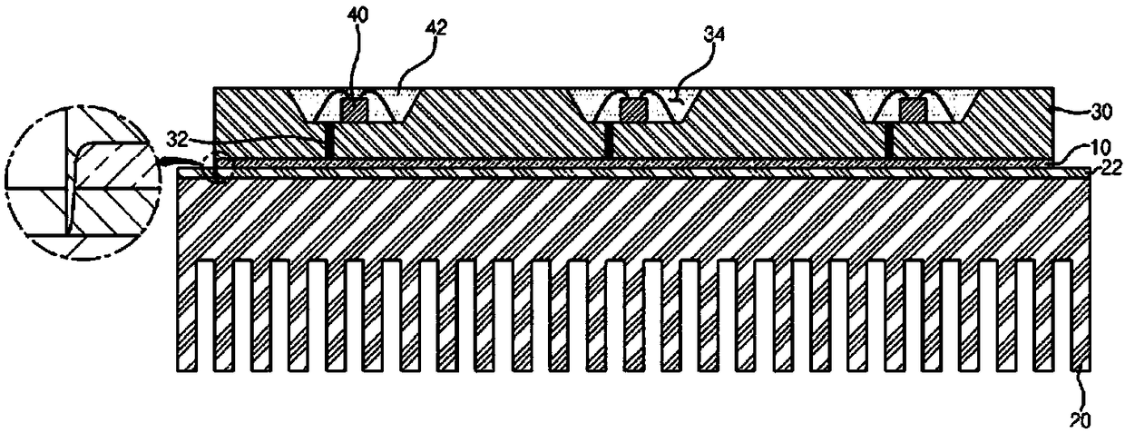
[0046] image 3 is a flowchart describing a method for manufacturing an optical device according to an exemplary embodiment of the present invention. Figures 4a to 4e is used to manufacture such as figure 2 The perspective view of the process in the main steps of the method of the optical device shown, and its cross-sectional view along the line A-A.

[0047] Such as image 3 As shown, according to the method for manufacturing an optical device according to an exemplary embodiment of the present invention, first, in step S10, a base substrate 100 for an optical device having at least one vertical insulating layer 110 (hereinafter referred to as " base substrate"), such as Figure 4a shown. exist Figure 4a and in subsequent figures, 120 denotes an optical...


PUM


Abstract

The present invention relates to an uncut chip substrate, and also relates to a method for manufacturing an optical device and to an optical device manufactured by the method, in which heat-dissipating performance by a heat sink and thermal insulation performance between a substrate and the heat sink are improved and workability is enhanced. According to a first characteristic of the present invention, the method for manufacturing an optical device comprises: (a) a step of preparing a disk for an optical device having a vertical thermal insulation layer; (b) a step of forming a groove along acut line formed on the lower surface of the disk for an optical device; (c) a step of applying liquid insulation material to the surface on which the groove is formed and hardening the liquid insulation material to form an electrically insulating layer having a planar surface; and (d) a step of forming a fixing hole penetrating in a vertical direction through both the disk for an optical device and the groove.

Description

[0001] This application is a divisional application of the PCT invention patent application with the application date of August 1, 2013, the application number 201380043437.7, and the title of the invention "Method for Manufacturing Optical Devices and Optical Devices Made by the Method". technical field [0002] The present invention relates to a method for manufacturing an optical device and an optical device manufactured by the method, and more particularly, to a method for manufacturing an optical device for improving heat dissipation performance through a heat sink, improving insulation performance between a substrate and a heat sink, and improving A method of manufacturability of an optical device, and an optical device manufactured by the method. Background technique [0003] In general, semiconductor light emitting diodes (LEDs) are attracting attention in various fields as environment-friendly light sources. In recent years, since the application of LEDs has expande...

Claims


Application Information

Patent Timeline
Patent Type & Authority Applications(China)
IPC IPC(8): H01L33/62H01L33/64
CPCH01L33/642H01L25/0753H01L2224/48091H01L2933/0075F21V19/003H01L2924/00014H01L33/647H01L2924/181H01L24/97H01L2224/48137H01L33/62H01L33/0095H01L2933/0066H01L2924/00012H01L33/48H01L33/52H01L33/64H01L33/644
Inventor 安范模南基明全永哲
Owner POINT ENG
Why Eureka
Try Eureka