Method for manufacturing memory device

A memory device and etching technology, applied in semiconductor/solid-state device manufacturing, electrical components, circuits, etc.

Active Publication Date: 2011-06-08
MACRONIX INT CO LTD
View PDF3 Cites 1 Cited by
  • Summary
  • Abstract
  • Description
  • Claims
  • Application Information

AI Technical Summary

Problems solved by technology

[0004] The present invention can overcome the defects of existing memory devices. An embodiment of the present invention provides a new method for manufacturing a memory device. The technical problem to be solved is to reduce the electrical short circuit between the word lines. very practical

Method used


Image

  • Method for manufacturing memory device
  • Method for manufacturing memory device
  • Method for manufacturing memory device

Examples


Embodiment Construction

[0041] In order to further explain the technical means and effects of the present invention to achieve the intended purpose of the invention, the specific implementation, structure and method of the method for manufacturing a memory device according to the present invention will be described below in conjunction with the accompanying drawings and preferred embodiments. , steps, features and effects thereof are described in detail below.

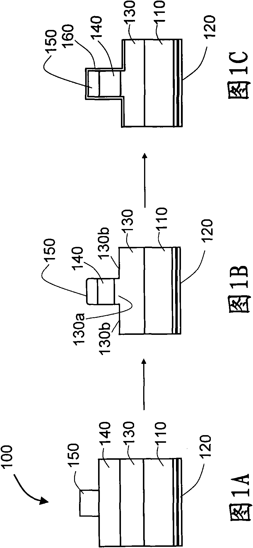
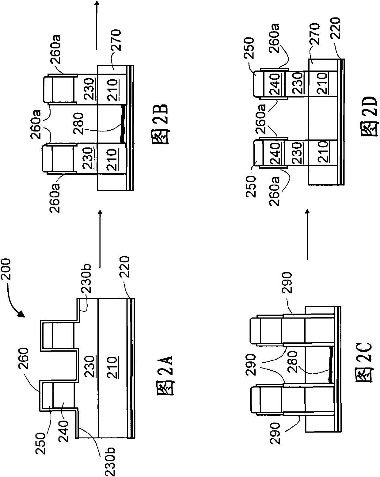
[0042] Now see the illustration, Figure 1A-Figure 1C It is an exemplary cross-sectional view of the method for manufacturing a memory device according to the first embodiment of the present invention. exist Figure 1A 100, a conductive layer portion of a word line is shown arranged 100 to provide a memory device. More specifically, a first polysilicon layer 110 is provided on an insulating structure 120 supported by the substrate. For example, the insulating structure 120 may comprise a multilayer stack of silicon oxide / silicon nitride / sil...


PUM


Abstract

The invention discloses a method for manufacturing a memory device, which comprises: providing a substrate with an insulation layer; forming first, second and third conducting layers on the insulation layer; forming a mask on the third conducting layer; etching by using the mask; providing an etched side wall part of the third conducting layer and the etched upper surface of the second conducting layer by the third conducting layer and the second conducting layer of a part of thickness; and forming a lining along the etched side wall part and the etched upper surface.

Description

technical field [0001] The present invention relates to a flash memory device, in particular to a method for manufacturing a memory device to reduce electrical shorts between word lines. Background technique [0002] In the traditional manufacturing process of flash memory devices, the polysilicon layer is usually etched to form word lines. However, etching polysilicon may create polysilicon residue between adjacent word lines. As a result, adjacent word lines are electrically connected resulting in an inoperable memory device due to these unnecessary polysilicon residues. As a result, there is a need to provide a new method for forming word lines that prevents the electrical connection of adjacent word lines and the generation of polysilicon residues. [0003] It can be seen that the above-mentioned existing memory device obviously still has inconveniences and defects in product structure, manufacturing method and use, and needs to be further improved urgently. In order ...

Claims


Application Information

Patent Timeline
Patent Type & Authority Applications(China)
IPC IPC(8): H01L21/768H01L21/8247H01L21/28
Inventor 李鸿志连楠梓陈光钊
Owner MACRONIX INT CO LTD
Why Eureka
Try Eureka