Method for controlling conductor length between through hole and welding disk of printed circuit board

A printed circuit board and wire length technology, applied in the electronic field, can solve the problems of PCB board error inspection and modification difficulties, more time and cost, and quality cannot be guaranteed, so as to improve product quality and work efficiency, avoid inspection and Effects of modification and shortening of design time

Inactive Publication Date: 2008-10-22
HUAWEI TECH CO LTD
View PDF1 Cites 0 Cited by
  • Summary
  • Abstract
  • Description
  • Claims
  • Application Information

AI Technical Summary

Problems solved by technology

[0009] Existing technical schemes use manual methods to route wires from pads to vias with a limited length. For all these wires, the operations of pulling wires, measuring and adjusting lengths need to be done manually. If the wires are accidentally modified after manual wiring The wires will not be found, and the inspection after the design is completed also needs to be carried out manually, so the efficiency is very low and the quality cannot be guaranteed, and it is very difficult to error check and modify a PCB board that has been designed, and it takes more time and effort. cost
[0010] Therefore, in practical application, the existing technical solutions have the following problems: low efficiency, unguaranteed quality, more design time and higher design cost

Method used


Image

  • Method for controlling conductor length between through hole and welding disk of printed circuit board
  • Method for controlling conductor length between through hole and welding disk of printed circuit board
  • Method for controlling conductor length between through hole and welding disk of printed circuit board

Examples


Embodiment Construction

[0043] In order to make the object, technical solution and advantages of the present invention clearer, the present invention will be further described in detail below in conjunction with the accompanying drawings.

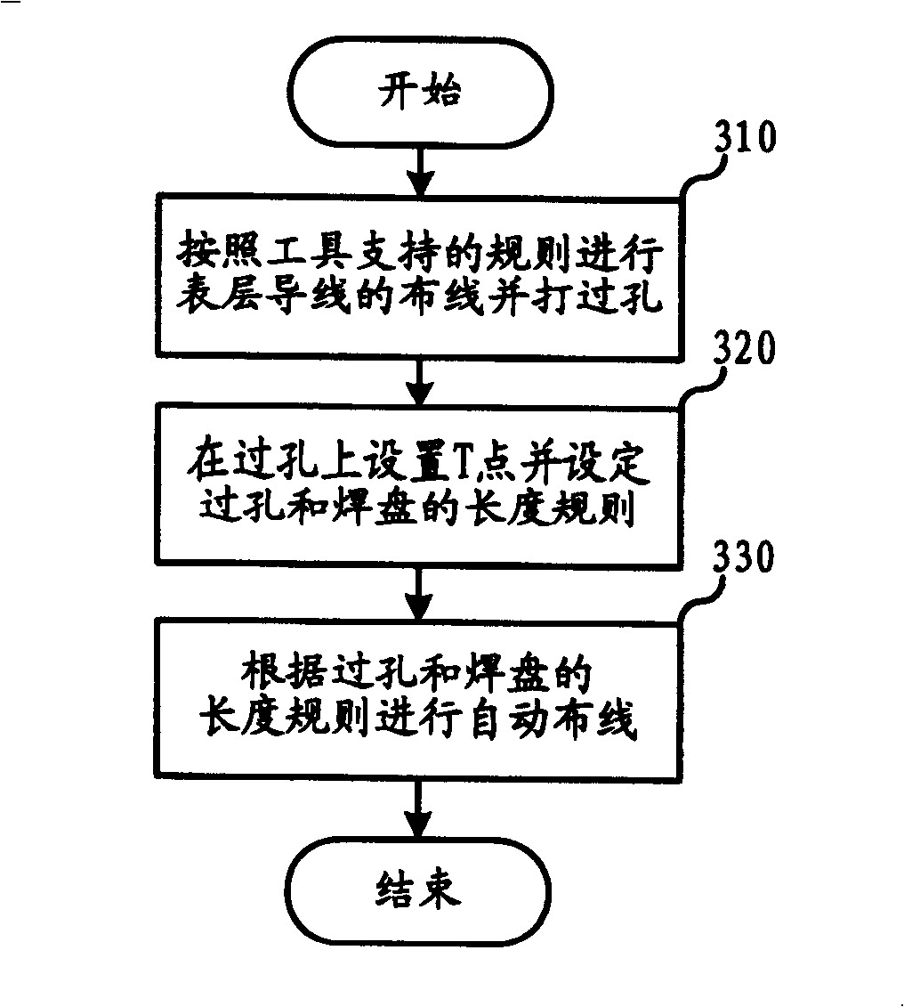
[0044]Considering that the EDA tool can automatically measure the distance from the T point to the pad, the solution of the present invention automatically adds the T point on the via hole, and sets constraint rules for each T point, and then the automatic routing function of the EDA tool can be used for routing , and finally you can check whether the wiring meets the requirements through the rule list. By using the solution of the invention, manual wiring is changed to automatic wiring, which will greatly help the improvement of PCB design efficiency and quality, facilitate inspection, shorten design time and reduce design cost.

[0045] According to the preferred embodiment of the present invention, the process of PCB via hole and wire length control between pad...


PUM


Abstract

This invention discloses a method for controlling lead length between the through holes and the weld plate of a PCB, which designs virtual points on the through hole and utilizes the character that the distance of the virtual point and the weld plate can be tested automatically to adjust the length of leads and provides a method for adjusting the lead length.

Description

technical field [0001] The invention relates to electronic technology, in particular to printed circuit board design technology in electronic technology. Background technique [0002] With the development of information technology, electronic devices are getting closer and closer to people's lives, and they appear in almost every corner of life. As an important component, a printed circuit board ("PCB" for short) appears in most electronic devices. In addition to fixing various electronic devices, the main function of the PCB is to provide mutual electrical connections for the various electronic devices on it. Those of ordinary skill in the art know that the substrate of the PCB is made of a material that is insulated from heat and is not easy to bend, and the circuit connection of the electronic device is provided through wires on the surface of the PCB. [0003] Various electronic devices can be directly soldered on the PCB board. In order to fix the device and ensure th...

Claims


Application Information

Patent Timeline
Patent Type & Authority Patents(China)
IPC IPC(8): G06F17/50
Inventor 黄希斌何波刘卫东
Owner HUAWEI TECH CO LTD
Why Eureka
Try Eureka