Trench DMOS transistor structure
A trench and gate trench technology, applied in the field of DMOS transistor manufacturing, can solve problems such as limiting the drain-source breakdown voltage of transistors
- Summary
- Abstract
- Description
- Claims
- Application Information
AI Technical Summary
Problems solved by technology
Method used
Image

Examples
Embodiment Construction
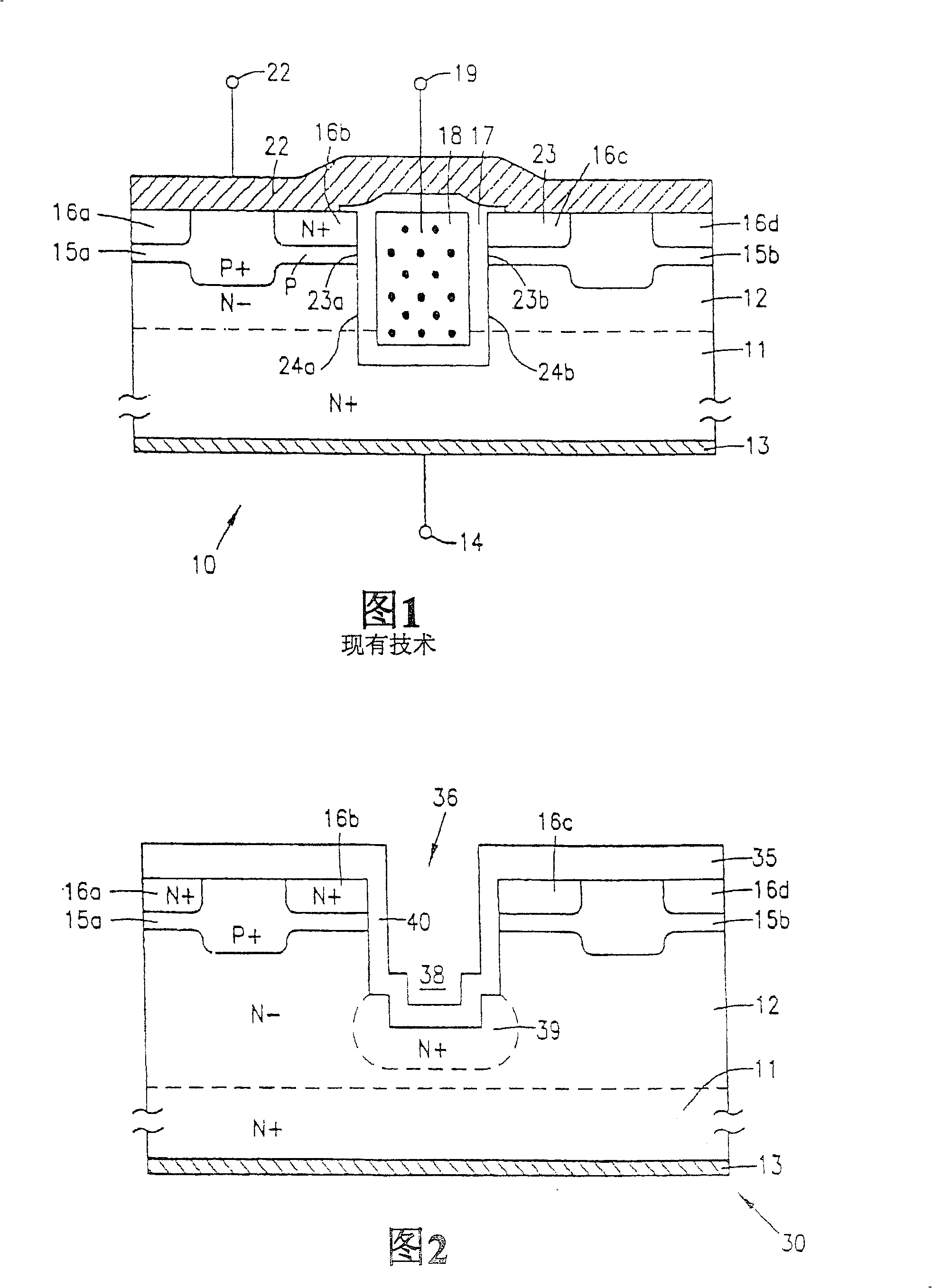
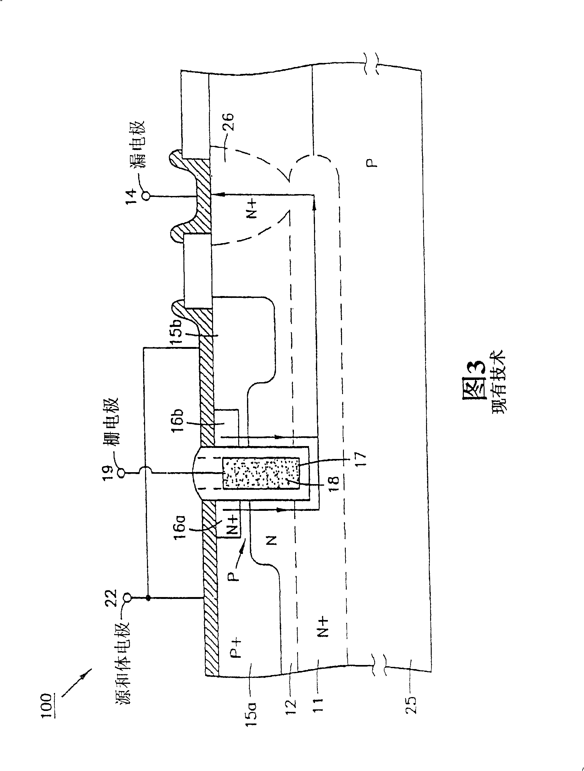
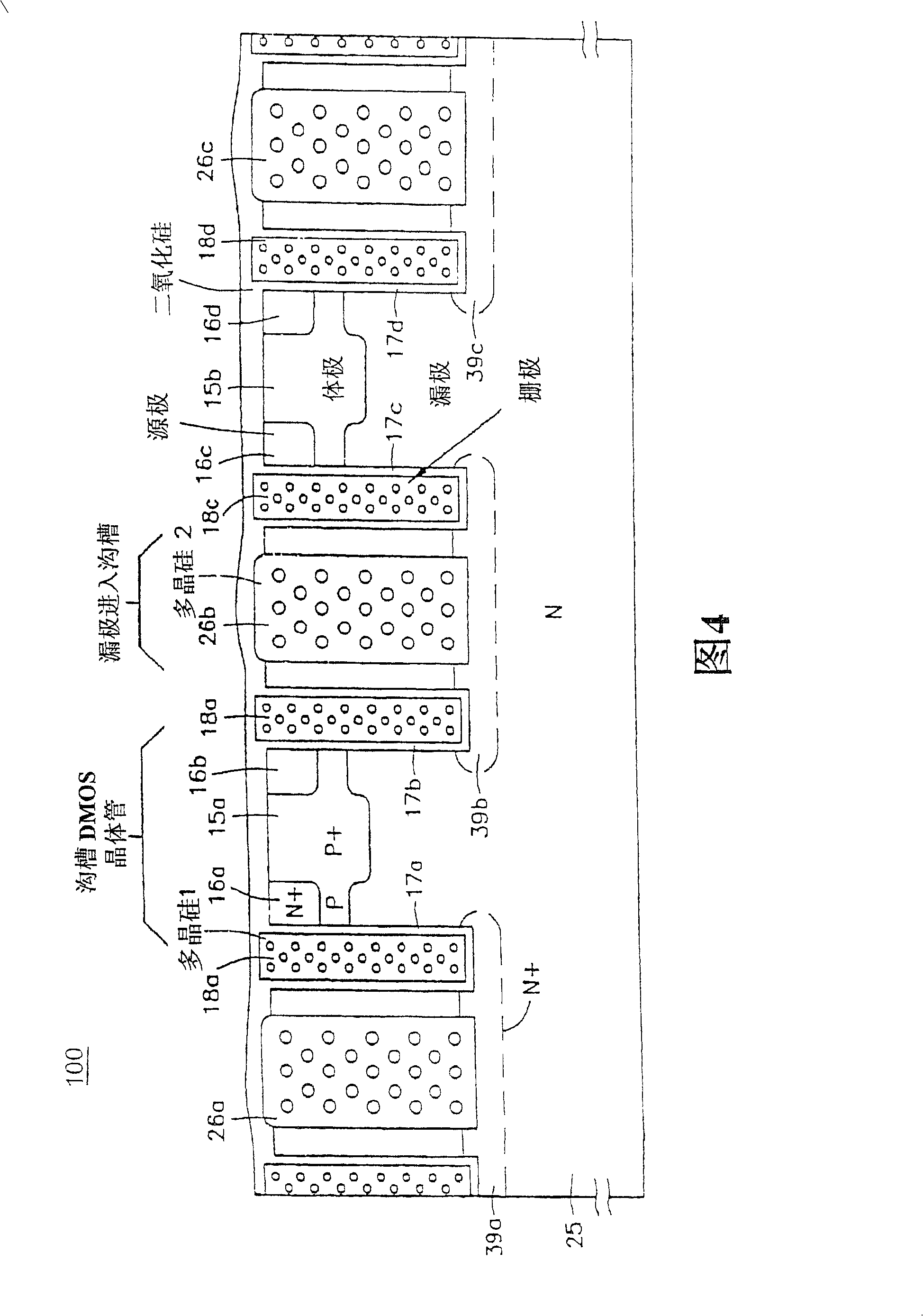
[0032] FIG. 3 shows a cross-sectional view of a trench DMOS transistor 100 constructed according to the prior art. A significant advantage of this structure is that it can be used not only in discrete components but also in integrated circuits because it is self-isolated. However, formation of buried layers and deposition of epitaxial layers are required. As shown in FIG. 3 , the trench DMOS transistor 100 includes a substrate 25 , a heavily doped buried region 11 and an epitaxial region 12 . The doping of the epitaxial region 12 is lighter than that of the buried region 11 . While substrate 25 may be N-type or P-type, a P-type substrate is typically preferred when the structure is to be incorporated into an integrated circuit because junction isolated devices can be easily fabricated. The DMOS transistor also includes source regions 16a and 16b and body regions 15a and 15b. As understood by those skilled in the art, body regions 15a and 15b may include deeper heavily doped ...
PUM
 Abstract
Description
Claims
Application Information