Light waveguide-layer inputting-outputting coupling interface assembly in EO-PCB board and its production

A technology of interface components and optical waveguides, which is applied in the direction of coupling of optical waveguides to achieve the effect of convenient assembly and convenient testing.

Inactive Publication Date: 2008-12-17
武汉海博光技术有限公司
View PDF4 Cites 0 Cited by
  • Summary
  • Abstract
  • Description
  • Claims
  • Application Information

AI Technical Summary

Problems solved by technology

At present, some papers have proposed the structure of the input and output interfaces, such as the free space coupling structure using a 45° mirror and a microlens array, etc., but these structures cannot strictly meet the above four requirements at the same time

Method used


Image

  • Light waveguide-layer inputting-outputting coupling interface assembly in EO-PCB board and its production
  • Light waveguide-layer inputting-outputting coupling interface assembly in EO-PCB board and its production
  • Light waveguide-layer inputting-outputting coupling interface assembly in EO-PCB board and its production

Examples


Embodiment Construction

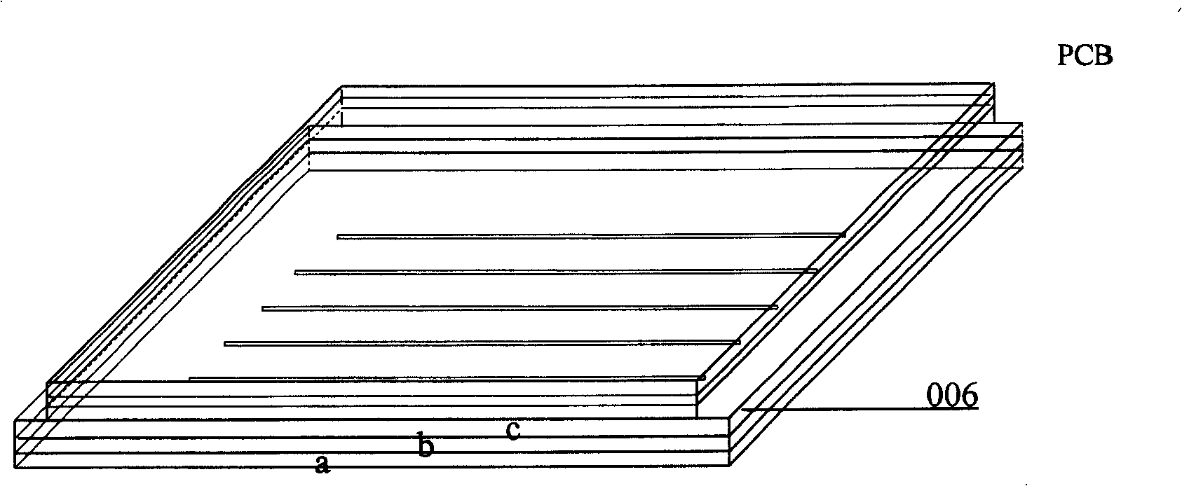
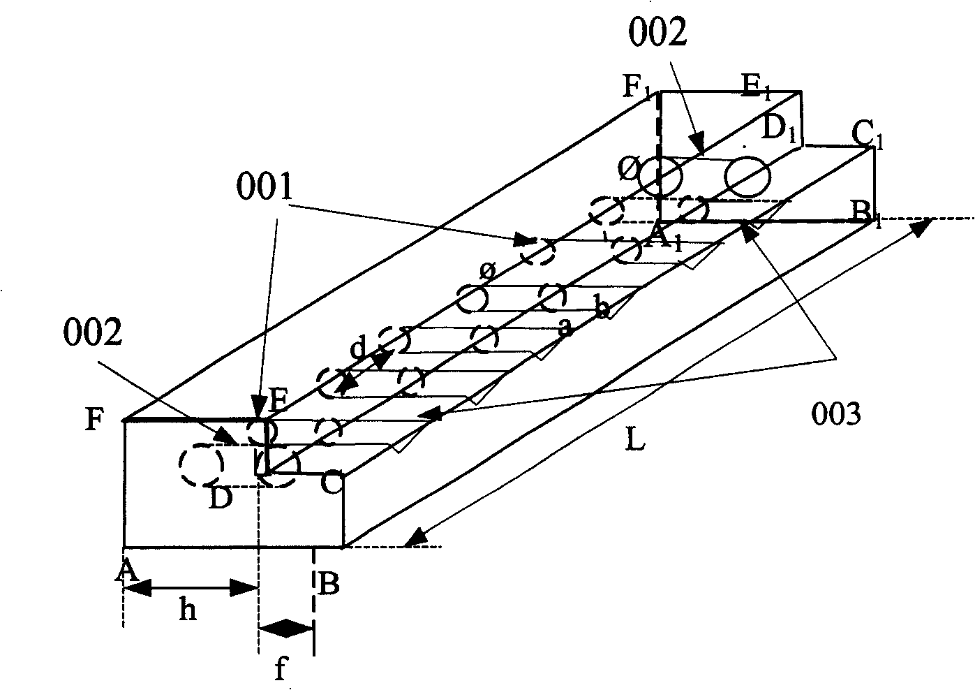
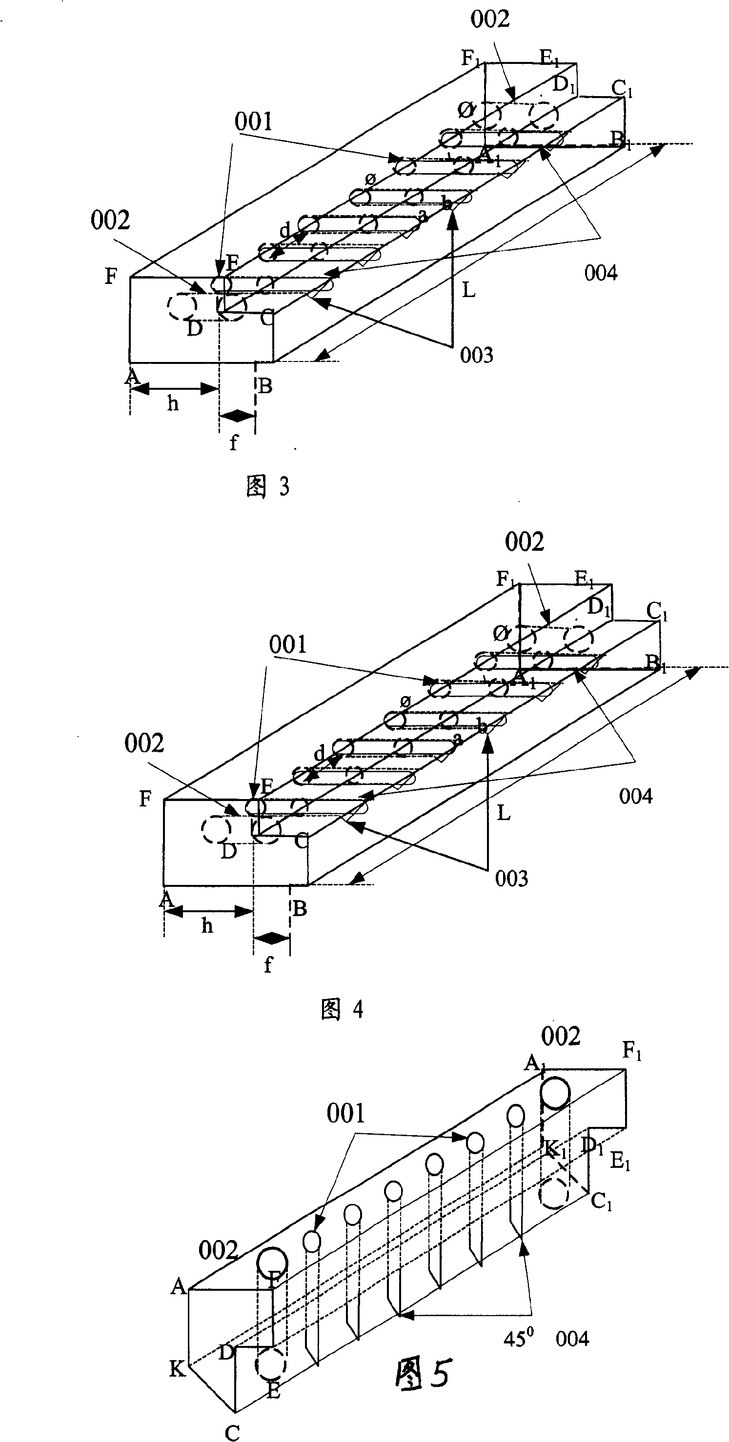
[0028] The optical waveguide layer input and output optical coupling interface assembly in the EO-PCB board of the present invention is an integrated module structure, such as figure 2shown. First design the mold, the plastic module produced by the mold has the following characteristics: the plastic module is a two-step ladder module, the side view is ABCDEF, and A1B1C1D1E1F1, divided into upper and lower steps, upper and lower steps The interface of the step surface is the central plane, and there are two types of through holes. The n through holes in the middle are optical fiber positioning holes 001, and the aperture diameter φ is about 126 μm. The two holes distributed on both sides are positioning pin holes 002, and the hole diameter Φ is about 0.7mm. These vias are centered at the interface DD of the second step 1 On the top, the upper and lower halves of the through hole are respectively in the upper and lower steps. On the surface of the lower step, along the outer...


PUM


Abstract

A method for preparing I / O light couple interface component of light waveguide layer in EO-PCB board includes using two-step from module as said component, setting through holes for positioning pin and optical fiber positioning at boundary position, cutting V-shape positioning groove at external tangent plane of surface on bottom step, placing optical fiber in said hole and said groove and injecting UV photochemical glue from port of each optical fiber, grinding two ends of optical fiber after curing, grinding one end to be 45 degree optical plane to optical fiber axle and another end to be optical plane vertical to optical fiber axle.

Description

technical field [0001] The invention relates to an input and output optical coupling interface component of an optical waveguide layer in an EO-PCB board and a preparation method. Background technique [0002] Due to the needs of aerospace, spaceborne, military modernization, and scientific and technological development, the next generation of information equipment must develop towards a T-bit level processing rate, and the processing rate between processors must be 10-40Gbps. The delay and bandwidth of signal interconnection are the key issues that must be solved first, and high-speed interconnection switching technology has become the top priority of high-performance computer system research. [0003] Although high-bandwidth electrical signal transmission has the advantages of relatively mature technology, easy interface implementation, high transmission bandwidth, small switching delay, and relatively low cost, due to the physical reasons of limited bandwidth of electrica...

Claims


Application Information

Patent Timeline
Patent Type & Authority Patents(China)
IPC IPC(8): G02B6/26
Inventor 曹明翠
Owner 武汉海博光技术有限公司
Why Eureka
Try Eureka