Silicon nanometer optical waveguide and optical fiber coupling and encapsulation method
A packaging method and optical waveguide technology, which is applied in the coupling of optical waveguides, can solve the problems of light diffraction leakage to the substrate, difficulty in device packaging, and strict requirements on the incident angle of optical fibers, so as to reduce interface reflection loss and accurately center alignment The effect of high efficiency and simple packaging process
Inactive Publication Date: 2010-11-10
SEMICON MFG INT (SHANGHAI) CORP +1
View PDF0 Cites 8 Cited by
- Summary
- Abstract
- Description
- Claims
- Application Information
AI Technical Summary
Problems solved by technology
The use of lensed fibers can reduce the fiber mode spot, but requires precise alignment with the waveguide, and it is almost impossible to directly align with the silicon nano-optical waveguide
The grating-assisted non-planar optical coupling method uses a one-dimensional or two-dimensional grating to approach the optical coupling from the direction perpendicular to the chip, which can realize optical coupling anywhere on the chip, but due to the diffraction leakage of light to the substrate and the gap between the grating and the optical fiber Mode mismatch requires DBR mirror substrate or inhomogeneous grating design, etc., and the wavelength-related properties of the grating determine that it cannot work with a wider bandwidth. The incident angle of the fiber is demanding, and the device packaging is difficult and the reliability is poor.
The mode spot converter can realize the transformation of the mode field size in the silicon nano-optical waveguide. The manufacturing process of the positive tapered mode spot converter is complicated and requires a longer size gradient waveguide; the reverse tapered mode spot converter can better integrate with CMOS The process is compatible, but the coupling loss is large, and the precise alignment of the optical fiber is still required, and the reliable coupling and packaging of the waveguide and the optical fiber cannot be achieved
V-shaped grooves are commonly used as a reference for aligning and fixing optical fibers, but simple V-shaped grooves cannot meet the requirements of efficient optical coupling and reliable packaging between silicon nano-optical waveguides and optical fibers
Method used
View moreImage
Smart ImageViewing Examples

Examples
Embodiment Construction
Login to View More PUM
 Abstract
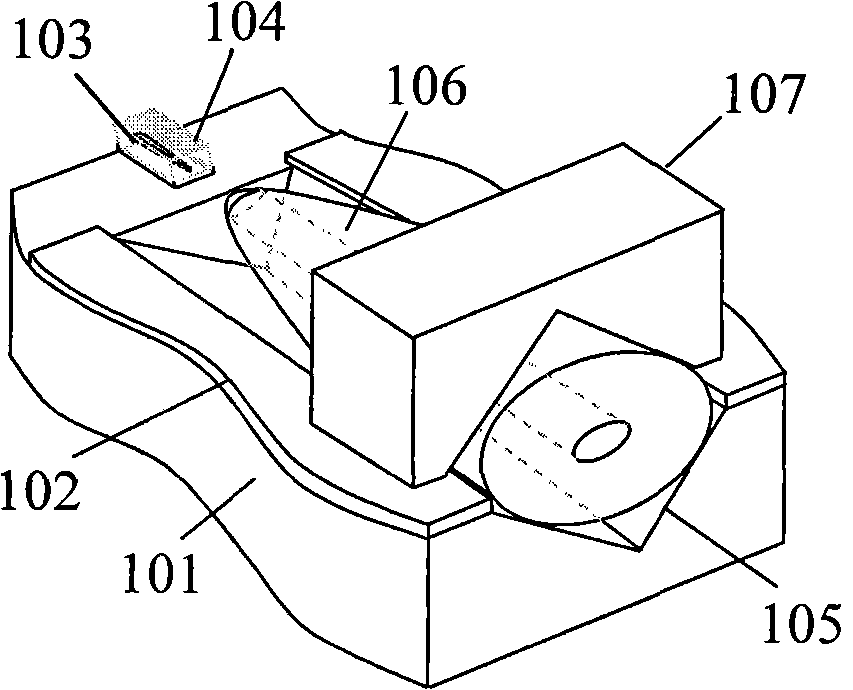
The invention relates to a silicon nanometer optical waveguide and optical fiber coupling and encapsulation method in the technical field of optical integrated chip coupling and encapsulation. In order to realize the high efficiency optical coupling and easy encapsulation of silicon optical waveguide and optical fiber, the invention provides the silicon nanometer optical waveguide and optical fiber coupling and encapsulation method. A back taper spot-size converter is used to realize the conversion from a small-sized spot-size in the silicon nanometer optical waveguide to a big-sized spot-size of the optical fiber; and the alignment coupling and the easy encapsulation of the silicon nanometer optical waveguide and the optical fiber is realized through the selfalignment characteristic of aV-shaped optical fiber positioning notch. The high efficiency of the back taper spot-size converter, the broadband optical coupling characteristic and the optical mode field size conversion capability are integrated with the SOI substrate characteristic and the V-shaped optical fiber positioning notch so as to realize the accurate central alignment and high efficiency optical coupling of the waveguide and the optical fiber; and in addition, the optical fiber fixing and encapsulation process is easy and convenient and is quite suitable for the application of actual production.
Description
A coupling packaging method of silicon nano-optical waveguide and optical fiber technical field The invention relates to the technical field of coupling and packaging of optical integrated chips, in particular to a method for coupling and packaging silicon nanometer optical waveguides and optical fibers. Background technique Silicon materials are transparent in the optical communication frequency bands with light wavelengths of 1.31 μm and 1.55 μm, and the high refractive index difference between Si (silicon) and SiO2 (silicon dioxide) makes silicon based on SOI (silicon-on-insulator) substrates The waveguide has a strong confinement effect on the optical field, and can be confined within a Si waveguide of several hundred nanometers. It can be made into a multifunctional, miniaturized, and high-density integrated photonic device. At the same time, it is compatible with the CMOS process and can realize photonic devices and The advantages of electronic device integration hav...
Claims
Login to View More Application Information
Patent Timeline
 Patent Type & Authority Patents(China)
IPC IPC(8): G02B6/26
Inventor 申华军周静涛刘新宇吴德馨
Owner SEMICON MFG INT (SHANGHAI) CORP