Novel hybrid integration method

A hybrid integration and new method technology, applied in the field of optical integration, can solve problems such as end face reflection and three-dimensional alignment error, affecting coupling efficiency, affecting device performance, etc., to reduce optical loss and optical reflection, increase alignment tolerance, The effect of efficient optical coupling

Inactive Publication Date: 2022-01-04
HUAZHONG UNIV OF SCI & TECH
View PDF2 Cites 0 Cited by
  • Summary
  • Abstract
  • Description
  • Claims
  • Application Information

AI Technical Summary

Problems solved by technology

[0004] However, the biggest problem of flip-chip integration at present is the coupling of light between different material systems.
Grating coupling (Grating coupling) cannot meet the working requirements of the entire C-band; mirror coupling (Mirror coupling) is difficult to process, and generally can only be produced at the end of the chip (Noriki A, Amano T, Shimura D, et al. Broadband and polarization- independent efficient vertical optical coupling with 45°mirror for optical I / O of Si photonics[J].Journal of Lightwave Technology,2016,34(3):978-984.); the coupling efficiency of direct docking coupling (Butt coupling) is limited on end face quality, end face reflection and 3D alignment error
Today's commercial Flip-chip platform can achieve alignment errors within 500nm in both horizontal directions through alignment marks, but alignment in the vertical direction is still a challenge, requiring high substrate thickness and uniformity of material etching. Moreover, different materials have different thermal expansion coefficients, and temperature changes will inevitably cause misalignment in the vertical direction of the optical docking part of the hybrid integrated device.
On the other hand, now more spot converters are used to enlarge the alignment spot, which is beneficial to direct docking to a certain extent, but there is always a gap between the end faces, which affects the coupling efficiency, and the three-dimensional alignment tolerance is not good. High, the theoretical optical coupling loss within the alignment error of ±1μm is -2.3dB (Theurer M, Moehrle M, Sigmund A, etal. Flip-chip integration of InP and SiN [J]. IEEE Photonics Technology Letters, 2019, 31 (3):273-276.)
In addition, how to reduce the light reflection of the end surface when the waveguide is directly connected is also a problem. Whether it is an etching interface or a cleavage surface, there will be a certain amount of end surface light reflected back to the active device, which will seriously affect the performance of the device. On-chip integrated optical isolator it's not easy either

Method used


Image

  • Novel hybrid integration method
  • Novel hybrid integration method
  • Novel hybrid integration method

Examples


Embodiment 1

[0035] refer to Figure 1-12 , the present invention provides a new hybrid integration method, comprising the following steps:

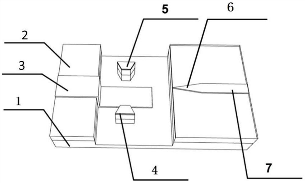
[0036] Assembling the motherboard chip; the motherboard chip includes a motherboard chip body, the motherboard chip body is provided with a motherboard chip metal area 3, the motherboard chip vertically supports the assembly and the motherboard chip waveguide area, and the motherboard chip waveguide area contains Coupled motherboard chip coupling waveguide region 6;

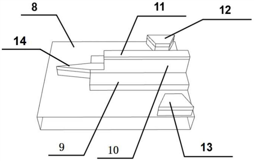
[0037] Assembling the daughterboard chip; the daughterboard chip includes a daughterboard chip body, the daughterboard chip body is provided with a daughterboard chip metal area 11, the daughterboard chip vertical support assembly and the daughterboard chip waveguide area, the daughterboard chip waveguide area contains the daughterboard chip coupling waveguide region 14;

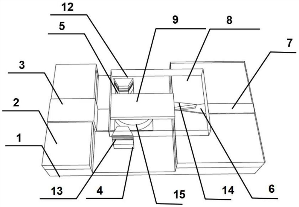
[0038] Assemble the integrated chip; the daughter board chip is bonded upside down on the top of the mother board...

Embodiment 2

[0074] According to attached Figure 13 As shown, in the second embodiment, on the basis of the first embodiment, the silicon-based waveguide chip is used as the daughter board chip, and the InP-based chip is used as the optical motherboard chip, which is opposite to the configuration of the mother-daughter chip in the first embodiment. The motherboard chip includes a motherboard chip body and a motherboard chip coupling area, the motherboard chip body includes a motherboard chip heat sink 25, and the top of the motherboard chip heat sink 25 is sequentially provided with an InP-based chip substrate 26, and an InP-based chip core layer 27. InP-based chip cover layer 28, InP-based chip metal area 29; the motherboard chip coupling area includes an InP-based chip coupling waveguide area 30; the motherboard chip is provided with a motherboard chip vertical support assembly, and the motherboard chip vertical support assembly includes But not limited to the fifth supporting member 31...


PUM

PropertyMeasurementUnit
Thicknessaaaaaaaaaa
Thicknessaaaaaaaaaa
Thicknessaaaaaaaaaa

Abstract

The invention discloses a novel hybrid integration method, which comprises the following steps of: assembling a mother board chip; assembling a daughter board chip; and assembling an integrated chip. The mother board chip comprises a mother board chip body, wherein the mother board chip body has a mother board chip metal area, a mother board chip vertical supporting assembly and a mother board chip waveguide area, and the mother board chip waveguide area comprises a coupling waveguide area used for vertical coupling. The daughter board chip comprises a daughter board chip body, wherein the daughter board chip body has a daughter board chip metal area, a daughter board chip vertical supporting assembly and a daughter board chip waveguide area, and the daughter board chip waveguide area comprises a coupling waveguide area. The daughter board chip is attached to the top end of the mother board chip in an inverted mode, the mother board chip vertical supporting assembly is attached to the daughter board chip vertical supporting assembly, the mother board chip coupling waveguide area is attached to or close to the daughter board chip coupling waveguide area, and the mother board chip metal area is fixedly connected with the daughter board chip metal area. According to the hybrid integration method, the alignment tolerance between the optical chips is increased, and the optical loss and the optical reflection are reduced.

Description

technical field [0001] The invention relates to the technical field of optical integration, in particular to a new hybrid integration method. Background technique [0002] In recent years, integrated optical circuits have developed rapidly. Integrating lasers, modulators, and detectors in optical fiber communications on a single chip can meet the development trend of miniaturization, low power consumption, and low cost. At present, integrated optical circuits can rely on many material systems. For example, active devices mainly come from indium phosphide, gallium arsenide, and gallium nitride, and passive devices mainly rely on silicon, silicon nitride, silicon oxide, aluminum nitride, and niobium. Lithium Oxide etc. Considering the wafer cost and mature processing technology, silicon has become the most promising material for integrated optical circuits. But silicon still can't meet all the needs of optical communication devices. For example, as a semiconductor material ...

Claims


Application Information

Patent Timeline
IPC IPC(8): G02B6/12
CPCG02B6/12G02B2006/12147G02B2006/12166G02B6/1228G02B6/423G02B6/4232G02B6/12002G02B6/136G02B6/13H05K1/144H05K3/368H05K2201/041
Inventor 国伟华戴向阳陆巧银
Owner HUAZHONG UNIV OF SCI & TECH
Why Eureka
Try Eureka