Mode spot converter coupled with optical fiber and optical waveguide and manufacturing method thereof
An optical waveguide and optical waveguide technology, applied in the field of optical communication, can solve problems such as difficulty in further improving coupling efficiency, complex coupler structure and process, and high processing cost, and achieve expanded application range, high universality, and large alignment tolerance Effect
- Summary
- Abstract
- Description
- Claims
- Application Information
AI Technical Summary
Problems solved by technology
Method used
Image
Examples
Embodiment 1
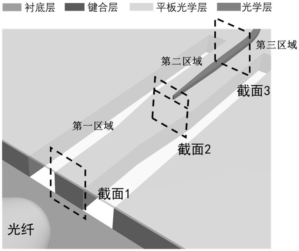
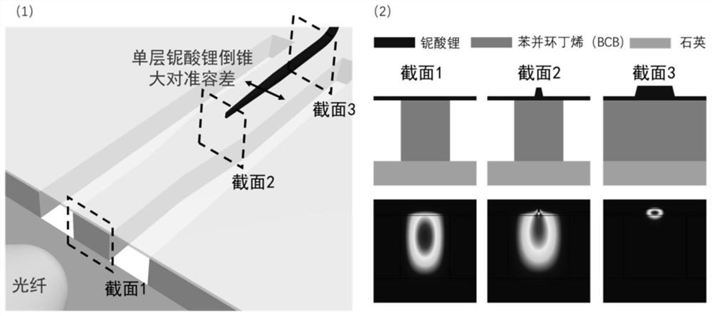
[0058] Prepare a quartz crystal in advance as the subsequent substrate, and prepare a thin-film lithium niobate wafer with a chromium sacrificial layer. The materials of the wafer from bottom to top are silicon or silicon dioxide substrate, silicon dioxide layer , a metal sacrificial layer (such as a chromium layer) and a thin-film lithium niobate layer; UV lithography exposure and development to obtain a BCB waveguide, and use the BCB layer as a bonding layer to bond the thin-film lithium niobate wafer to the quartz crystal; after the bonding is completed , by metal etching solution (such as chromium etching solution), the substrate part of the thin-film lithium niobate wafer is peeled off; the etching pattern of thin-film lithium niobate is formed by electron beam exposure; and then RIE is etched by reactive plasma Obtain a single-layer inverted-taper lithium niobate waveguide, and finally perform scribing and waveguide end face polishing at the preset position of the bonding...
Embodiment 2
[0066] A 300nm-thick thin-film lithium niobate wafer with a chromium sacrificial layer is bonded to a standard SOI waveguide through the above-mentioned process to realize the heterogeneous integration of lithium niobate and silicon base, in which the thickness of BCB used for bonding can be flexibly adjusted . Compared with the existing solution of heterogeneous integration through BCB thin layer, the thickness of BCB in this application is relatively thick, and there is no need to strictly control the thickness, which reduces the difficulty of the process. The silicon-based waveguide needs to form a taper in the coupling region to gradually couple the light in the silicon waveguide into the tapered BCB waveguide above the silicon waveguide, and then couple the light to the single-layer inverted cone above the BCB waveguide through the tapered BCB waveguide In the lithium niobate ridge waveguide, finally transition to the normal single-mode lithium niobate ridge waveguide. T...
Embodiment 3
[0068] Compared with the two-stage BCB tapered waveguide and tapered lithium niobate waveguide in Embodiment 1, the linear tapered waveguide of BCB and lithium niobate can be replaced by a tapered waveguide that changes in a parabolic or exponential or sinusoidal shape Perform parameter optimization design to obtain better performance and further reduce device size.
PUM
| Property | Measurement | Unit |
|---|---|---|
| thickness | aaaaa | aaaaa |
| depth | aaaaa | aaaaa |
| thickness | aaaaa | aaaaa |
Abstract
Description
Claims
Application Information
 - R&D
- Intellectual Property
- Life Sciences
- Materials
- Tech Scout
- Unparalleled Data Quality
- Higher Quality Content
- 60% Fewer Hallucinations
Browse by: Latest US Patents, China's latest patents, Technical Efficacy Thesaurus, Application Domain, Technology Topic, Popular Technical Reports.
© 2025 PatSnap. All rights reserved.Legal|Privacy policy|Modern Slavery Act Transparency Statement|Sitemap|About US| Contact US: help@patsnap.com


