Silicon-based integrated optical isolation device based on topology protection mechanism

A technology of topology protection and optical isolation, which is applied in the field of integrated optics, can solve problems such as the inability to realize optical communication bands and non-trivial topological boundary states, and achieve the effects of good scalability, good locality, and improved processing tolerances

Active Publication Date: 2020-03-31
UNIV OF ELECTRONICS SCI & TECH OF CHINA
View PDF4 Cites 12 Cited by
  • Summary
  • Abstract
  • Description
  • Claims
  • Application Information

AI Technical Summary

Problems solved by technology

[0010] In view of the above-mentioned problems, in order to solve the technical problem that the existing optical isolation devices cannot realize non-trivial topologica...

Method used


Image

  • Silicon-based integrated optical isolation device based on topology protection mechanism
  • Silicon-based integrated optical isolation device based on topology protection mechanism
  • Silicon-based integrated optical isolation device based on topology protection mechanism

Examples


Embodiment Construction

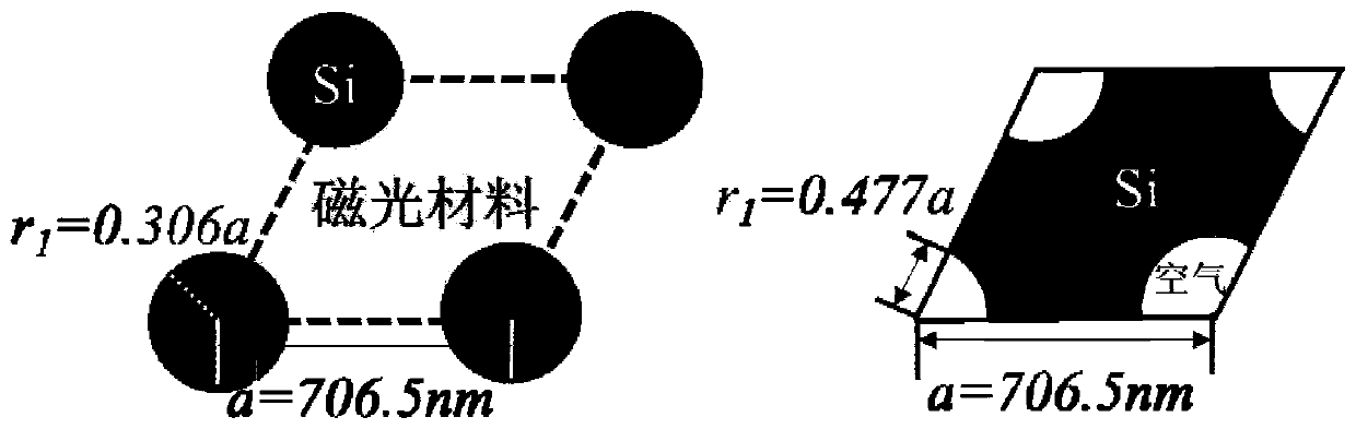
[0031] As mentioned in the background section, due to the lack of magneto-optical materials with strong magneto-optic effects in the optical communication frequency domain, non-trivial topological boundary states are difficult to achieve in the optical communication band. Therefore, the development of silicon-based integrated optical isolation devices based on topological protection mechanisms based on materials with weak magneto-optic effects is of great significance for the monolithic integration of magneto-optical isolators. In addition, due to the traditional TE mode polarization design MZI, MMI and other isolators need to deposit magneto-optical materials on the side walls, the process is difficult and the device performance is poor.

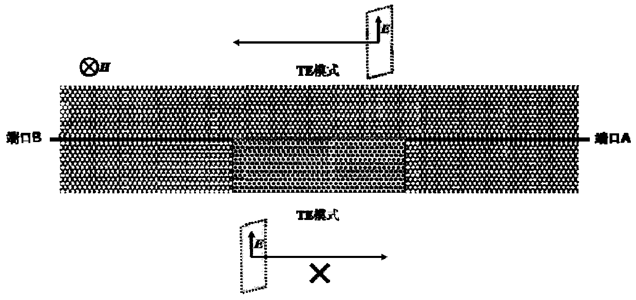
[0032] The invention adopts the energy band design method of the photonic crystal to adjust the boundary state energy band of the photonic crystal to conveniently obtain the isolation device of TE mode polarization, realize the optical isola...


PUM


Abstract

The invention belongs to the field of integrated optics, and particularly relates to a silicon-based integrated optical isolation device based on a topology protection mechanism. By adjusting the boundary states of the linear defect photonic crystal module and the topological non-uniform low group velocity photonic crystal module, the excitation and coupling regulation and control of the low groupvelocity boundary state are realized. According to the invention, the line defect photonic crystal waveguide with low group velocity is used as a transition coupling structure, so that the group velocity is matched while the coupling loss is reduced. The boundary state propagated in the photonic crystal has low group velocity and good locality, so that the size of the device is greatly reduced, and the loss is low; an isolator of TE polarization can be conveniently obtained; and in addition, steep bending transmission can be obtained through design. The invention provides a new mechanism of the optical isolation device; the processing tolerance can be obviously improved, and the stability and the expansibility are good; the design may be on-chip integrated using a semiconductor process.

Description

technical field [0001] The invention belongs to the field of integrated optics, in particular to a silicon-based integrated optical isolation device based on a topology protection mechanism. Background technique [0002] The optical isolator integrated on the chip in integrated optics has the characteristics of one-way conduction, which can suppress optical communication, and the reflected light in the optical interconnection system enters the laser, which significantly reduces the intensity and phase noise of the device. Traditional optical isolators are usually discrete devices, which are bulky, expensive to manufacture, and difficult to integrate. They cannot be mass-produced at low cost by using semiconductor production methods like non-reciprocal devices in circuits. [1] . [0003] Topological photonics provides new ideas for the development of integrated optical isolators. Topological photonics is an emerging discipline that combines traditional optical research with ...

Claims


Application Information

Patent Timeline
IPC IPC(8): G02F1/09G02B1/00
CPCG02B1/005G02F1/093
Inventor 毕磊杨玉聪秦俊邓龙江
Owner UNIV OF ELECTRONICS SCI & TECH OF CHINA
Why Eureka
Try Eureka