High-speed high-response photoelectric detector and manufacturing method thereof

A technology of photodetector and manufacturing method, applied in circuits, electrical components, semiconductor devices, etc., can solve problems such as increasing the difficulty of alignment and packaging, difficult testing and packaging, etc., reducing device capacitance, improving device bandwidth, The effect of efficient optical coupling

Pending Publication Date: 2022-02-08
南京中电芯谷高频器件产业技术研究院有限公司
View PDF4 Cites 0 Cited by
  • Summary
  • Abstract
  • Description
  • Claims
  • Application Information

AI Technical Summary

Problems solved by technology

However, the disadvantage of the back-illuminated photodetector is that it is difficult to test and package: an additional flip-chip welding process is required during testing and packaging, and the detector is welded on another substrate; in addition, due to the existence of the remaining InP substrate, in order to realize Higher optical coupling efficiency requires the integration of silicon lenses on the surface of the InP substrate, which further increases the difficulty of alignment and packaging

Method used


Image

  • High-speed high-response photoelectric detector and manufacturing method thereof
  • High-speed high-response photoelectric detector and manufacturing method thereof
  • High-speed high-response photoelectric detector and manufacturing method thereof

Examples


Embodiment 1

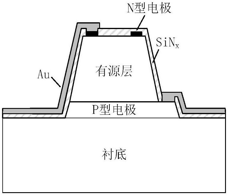
[0033] This embodiment provides a high-speed and high-response photodetector with a structure such as figure 1 As shown, including substrate, P-type electrode, active layer and N-type electrode.

[0034] In the embodiment of the present invention, the substrate is single crystal silicon, the P-type electrode is metal Ti / Pt / Au, and the N-type electrode is metal AuGeNi / Au.

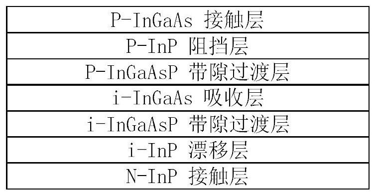
[0035] In the embodiment of the present invention, the active layer of the detector is as follows from bottom to top: P-InGaAs contact layer, P-InP barrier layer, P-InGaAsP band gap transition layer, i-InGaAs absorption layer, i-InGaAsP band gap transition layer , i-InP drift layer and N-InP contact layer.

[0036] Specifically, the i-InGaAs absorption layer has a thickness of 600 nm, and the i-InP drift layer has a thickness of 300 nm.

[0037] In addition, in the embodiment of the present invention, there is a SiNx anti-reflection film on the active layer of the detector with a thickness of 200 nm.

Embodiment 2

[0039] This embodiment provides a method for fabricating a high-speed and high-response photodetector, including the following steps:

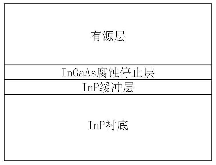
[0040] Step 1, such as figure 2 As shown, an InP buffer layer, an InGaAs etch stop layer and a detector active layer are sequentially grown on an InP substrate, and the detector active layer is as image 3 Shown, from bottom to top are: N-InP contact layer, i-InP drift layer, i-InGaAsP bandgap transition layer, i-InGaAs absorption layer, P-InGaAsP bandgap transition layer, P-InP barrier layer and P -InGaAs contact layer; Specifically, the thickness of the grown InGaAs corrosion stop layer is 500nm, the thickness of the i-InP drift layer is 300nm, and the thickness of the i-InGaAs absorption layer is 600nm;

[0041] Step 2. Evaporate P-type electrode Ti / Pt / Au on the P-InGaAs contact layer, evaporate metal Au on another single crystal silicon wafer, and bond the InP wafer and the silicon substrate wafer together by gold-gold thermocompression ...


PUM

PropertyMeasurementUnit
thicknessaaaaaaaaaa
thicknessaaaaaaaaaa
thicknessaaaaaaaaaa

Abstract

The invention discloses a high-speed high-response photoelectric detector and a manufacturing method thereof. The photoelectric detector comprises a substrate, a P-type electrode, an active layer and an N-type electrode, and the P-type electrode serves as a reflecting layer of incident light at the same time. The manufacturing method of the photoelectric detector comprises the following steps: growing an epitaxial layer on an InP substrate; evaporating a P-type electrode Ti / Pt / Au on the P-InGaAs contact layer, evaporating metal Au on the other substrate, and integrating the InP sheet and the other substrate sheet together through a gold-gold thermocompression bonding technology; removing the InP substrate; preparing an N electrode on the N-InP contact layer; corroding the active layer of the detector, and etching the P-type electrode; depositing a SiNx medium, and forming windows on the N-type electrode and the P-type electrode through etching; and manufacturing an Au electrode, and finally completing the preparation of the photoelectric detector. The photoelectric detector prepared through the preparation method has the advantages of being large in bandwidth, high in response and easy to couple and package.

Description

technical field [0001] The invention relates to the field of semiconductor devices, in particular to a high-speed and high-response photodetector and a manufacturing method thereof. Background technique [0002] Photodetectors can realize photoelectric conversion and are widely used in fields such as optical communication and laser radar. Bandwidth and responsivity are two important performance indicators of photodetectors. Compared with waveguide photodetectors, surface-incidence photodetectors are easier to achieve high-efficiency coupling with optical fibers; however, surface-incidence photodetectors have a contradiction between bandwidth and responsivity: when the thickness of the light-absorbing region is thinner , the shorter the carrier drift time, the faster the response rate of the device, but the smaller the device responsivity. [0003] The back-illuminated photodetector can alleviate the contradiction between the above-mentioned mutual constraints of bandwidth ...

Claims


Application Information

Patent Timeline
Patent Type & Authority Applications(China)
IPC IPC(8): H01L31/0224H01L31/105H01L31/18
CPCH01L31/022408H01L31/105H01L31/1844
Inventor 李冠宇戴家赟王宇轩牛斌
Owner 南京中电芯谷高频器件产业技术研究院有限公司
Why Eureka
Try Eureka