Printing circuit board

A technology for printed circuit boards and circuit layers, which is applied to printed circuit components, secondary processing of printed circuits, and printed electrical components, etc. It can solve problems such as electrical defects and achieve the effect of maintaining electrical quality

Inactive Publication Date: 2009-02-04
LITE ON IT
View PDF6 Cites 0 Cited by
  • Summary
  • Abstract
  • Description
  • Claims
  • Application Information

AI Technical Summary

Problems solved by technology

[0008] However, in the lead-free process test carried out with lead-free solder paste, it is known that the large copper foil layer 8 of the grounding area on the printed circuit board 2 commonly used will generally produce air bubbles 4, that is, some areas of the copper foil layer 8 will bulge. Bubbles form and separate from the substrate 6, so serious electrical defects will be formed

Method used


Image

  • Printing circuit board
  • Printing circuit board
  • Printing circuit board

Examples


Embodiment Construction

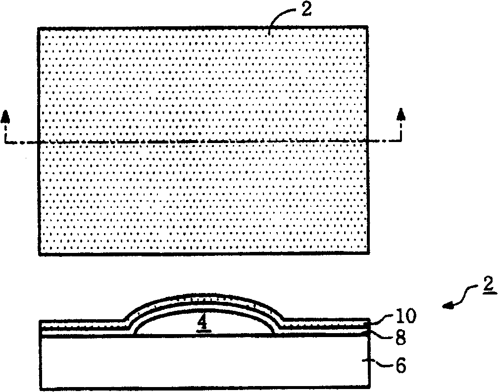
[0019] The invention relates to a printed circuit board (PCB). The source of the idea is that it can avoid air bubbles in the copper foil layer when the lead-free solder paste is used for surface mounting (SMT) in the manufacture of the board of the optical drive. , this printed circuit board is the substrate required for the board in the optical drive.

[0020] At present, the printed circuit board of the machine board used in the optical drive is provided with a layer of substrate and a circuit layer on the upper and lower surfaces respectively. The circuit layer is a conductive material, and copper foil is commonly used as the circuit layer, and the substrate is mostly FR1 substrate, CEM1 substrate, or CEM3 substrate. In this embodiment, copper foil will be used as the circuit layer, that is, the copper foil layer described below, to illustrate the relevant technical features of the present invention.

[0021] Such as figure 2 , figure 2 is a schematic diagram of the a...


PUM


Abstract

The invention has a circuit layer located on its baseplate surface and having grids. The circuit layer has even numbers of meshes by which the separation between the circuit layer and the baseplate can be avoided in the process of welding the electronic components. Meanwhile the circuit layer with grids can provide better anti-electromagnetic wave effect.

Description

technical field [0001] The invention relates to a printed circuit board, in particular to a printed circuit board which can withstand high temperature process. Background technique [0002] In the past when there was no awareness of environmental protection, various active and passive components and chips installed on the printed circuit board (Print Circuit Board; PCB) in the form of plug-in (DIP) or surface mount (SMT) were soldered with lead solder. Or use leaded solder paste to connect with the etched circuit on the surface of the printed circuit board by reflow to achieve the purpose of electrical connection. [0003] Taking the traditionally used leaded solder paste as an example, the content of tin and lead is 63% tin and 37% lead, its melting point is 183 degrees Celsius, and its maximum temperature in the reflow process must reach 210 degrees Celsius. In recent years, with the rising awareness of environmental protection, the European WEEE regulations require that ...

Claims


Application Information

Patent Timeline
Patent Type & Authority Patents(China)
IPC IPC(8): H05K3/38H05K1/16H05K1/02
Inventor 陈誉升
Owner LITE ON IT
Why Eureka
Try Eureka