Non-volatile memory system and method for programming and reading update data
A non-volatile storage and storage system technology, applied in the field of data storage systems
- Summary
- Abstract
- Description
- Claims
- Application Information
AI Technical Summary
Problems solved by technology
Method used
Image
Examples
Embodiment Construction
[0031] [Description of existing large block management technology]
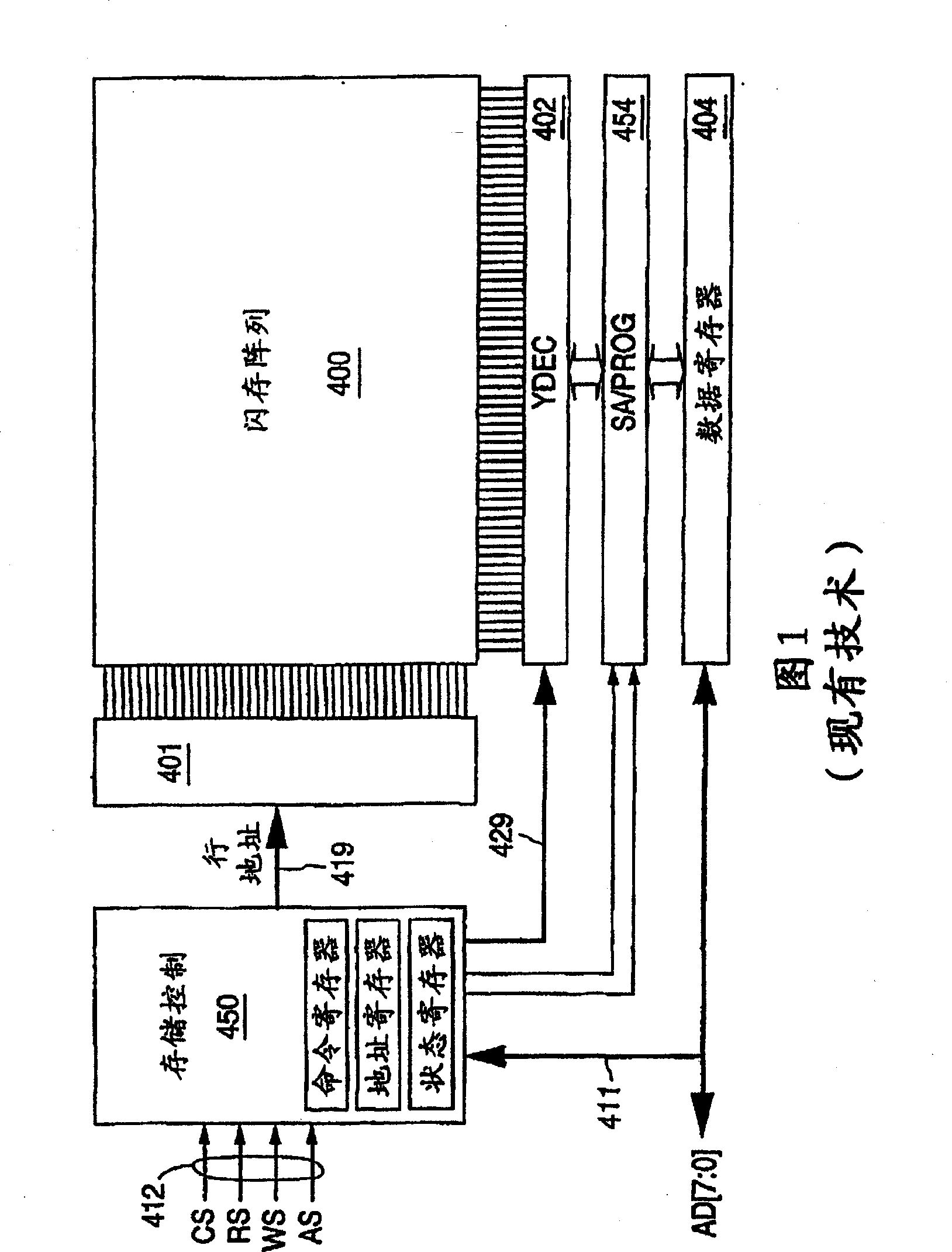
[0032] FIG. 1 shows the internal architecture of a typical flash memory device. The main components include: an input / output (I / O) bus 411 and control signals 412 for interfacing to an external controller; a memory control circuit 450 for controlling internal memory through registers for command, address, and status signals operate. Also included is one or more flash EEPROM partitioned arrays 400, where each array has its own row decoder (XDEC) 401 and column decoder (YDEC) 402, a set of sense amplifiers and program control circuitry (SA / PROG) 454 and data register 404. Currently, memory segments typically include one or more conductive floating gates as storage elements, but other long-term electronic charge storage elements may be used instead. Memory cell arrays can operate with two charge levels defined for each storage element, using each element to store one bit of data. Optionally, more than two s...
PUM
 Abstract
Description
Claims
Application Information


