Liquid crystal display device and its driving method

A liquid crystal display and thin film transistor technology, applied in the field of liquid crystal display and its drive, can solve the problems of long response time of liquid crystal display and achieve the effect of shortening the response time

Inactive Publication Date: 2009-07-22
INNOCOM TECH (SHENZHEN) CO LTD +1
View PDF5 Cites 0 Cited by
  • Summary
  • Abstract
  • Description
  • Claims
  • Application Information

AI Technical Summary

Problems solved by technology

[0007] In order to solve the problem of relatively long response time of liquid crystal displays in the prior art, the present invention provides a liquid crystal display capable of shortening the response time

Method used


Image

  • Liquid crystal display device and its driving method
  • Liquid crystal display device and its driving method
  • Liquid crystal display device and its driving method

Examples


Embodiment Construction

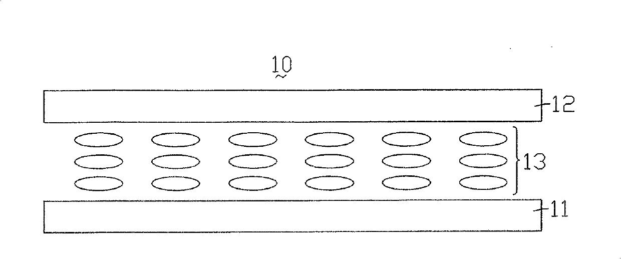
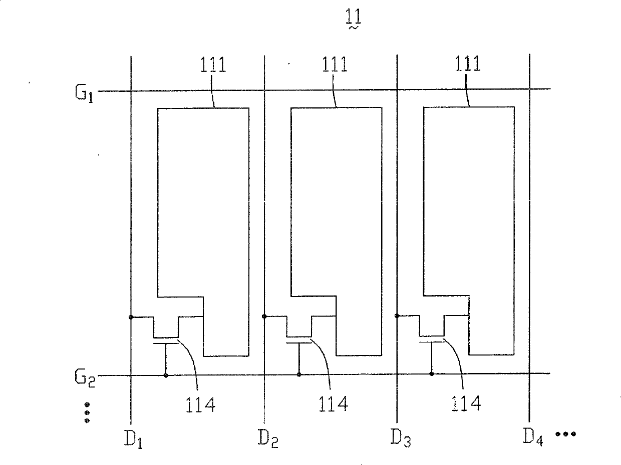
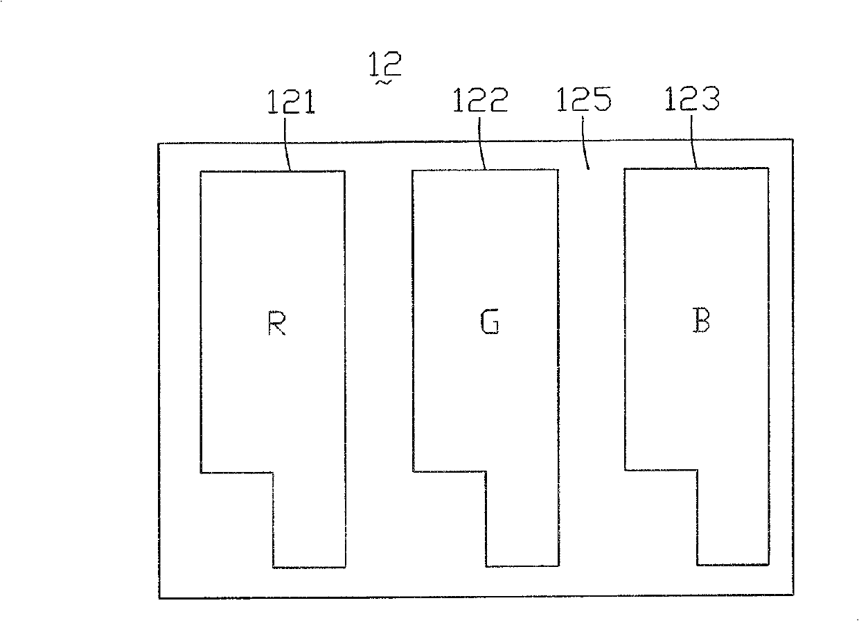
[0021] The liquid crystal display 20 of the present invention comprises a thin film transistor substrate 21, a color filter substrate 22 and a liquid crystal layer 23 sandwiched between the two, such as Figure 4 shown. The specific structures of the thin film transistor substrate 21 and the color filter substrate 22 are as follows: Figure 5 , Image 6 shown. The thin film transistor substrate 21 includes a plurality of parallel scanning lines G1, G2 (not shown in the figure), ..., and a plurality of rows of data lines D1, D2, D3 ... ... parallel to each other and perpendicular to the scanning lines. ...

[0022] The scanning line G1 divides the area surrounded by the data lines D1 and D2 into upper and lower parts. The upper part includes a first pixel electrode 311 and a first thin film transistor 321. The area of ​​the first pixel electrode 311 is close to the Area area, the first thin film transistor 321 is arranged adjacent to the scanning line G1 and the data line D...


PUM


Abstract

The invention provides a liquid crystal display which comprises a plurality of picture elements, a plurality of scanning lines and a plurality of datawires, wherein each picture element comprises a red sub-pixel, a green sub-pixel and a blue sub-pixel. The red sub pixel comprises a first red sub-pixel and a second red sub-pixel, the same scanning line provides sweep signals for the first and the second red sub-pixels, and two datawires respectively provide data voltage for the first and the second red sub-pixel. The green sub-pixel comprises a first green sub-pixel and a second green sub-pixel, the same scanning line provides sweep signals for the first green sub-pixel and the second green sub-pixel, and two datawires respectively provide data voltage for the first green sub-pixel and the second green sub-pixel. The blue sub-pixel comprises a first blue sub-pixel and a second blue sub-pixel, the same scanning line provides sweep signals for the first blue sub-pixel and the second blue sub-pixel, and two datawires respectively provide data voltage for the first blue sub-pixel and the second blue sub-pixel.

Description

technical field [0001] The invention relates to a liquid crystal display and a driving method thereof. Background technique [0002] The liquid crystal display 10 generally includes a thin film transistor substrate (TFT-Array Substrate) 11, a color filter substrate (Color-Filter Substrate) 12 and a liquid crystal layer 13 sandwiched between the two, as figure 1 shown. The specific structures of the thin film transistor substrate 11 and the color filter substrate 12 are as follows: figure 2 , image 3 shown. The thin film transistor substrate 11 includes a plurality of scan lines G1, G2... parallel to each other, a plurality of data lines D1, D2, D3... parallel to each other and perpendicular to the scan lines, a plurality of Pixel electrodes 111 distributed in the area divided by the scanning line and the data line, a plurality of thin film transistors 114 adjacent to the scanning line and the data line, the gates of the thin film transistors 114 are respectively electr...

Claims


Application Information

Patent Timeline
Patent Type & Authority Patents(China)
IPC IPC(8): G02F1/133G02F1/1362G02F1/1335G09G3/36
CPCG09G2300/0443G02F2001/134345G09G2310/061G09G3/3648G09G2320/0252G02F1/134345
Inventor 陈英泰
Owner INNOCOM TECH (SHENZHEN) CO LTD
Why Eureka
Try Eureka