

Manufacturing method for electronic device
A technology for electronic devices and manufacturing methods, applied in semiconductor/solid-state device manufacturing, circuits, electrical components, etc., can solve problems such as disconnection reliability, and achieve the effect of eliminating equipment investment and reducing costs
- Summary
- Abstract
- Description
- Claims
- Application Information
AI Technical Summary
Problems solved by technology
Method used
Image

Examples
no. 1 approach
[0065] (electronic device)
[0066] Next, the present invention will be described in detail.
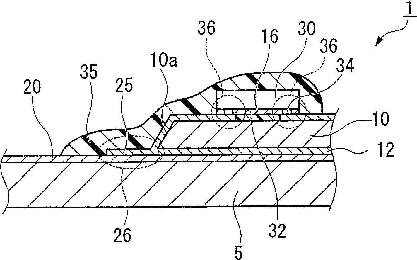
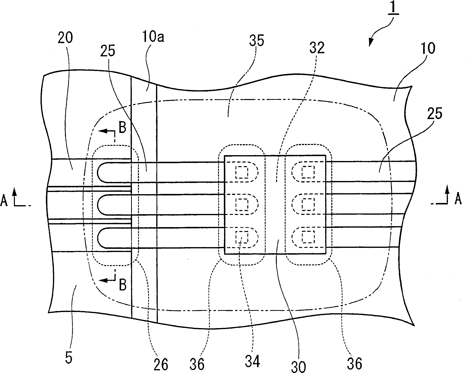
[0067] figure 1 It is a figure which shows and explains the electronic device manufactured using the manufacturing method of the electronic device of this invention, and is figure 2 The side sectional view of A—A line looking down. figure 1 Among them, symbol 1 is the electronic device of the present invention. figure 2 It is a plan view showing a part of the electronic device 1 (resin 35 described later) seen through from a vertical direction, and is a diagram for explaining the electronic device 1 of the present invention.
[0068] Such as figure 1 As shown, the electronic device 1 includes, for example, a substrate 5 made of Si and a pedestal 10 formed on the substrate. The above-mentioned pedestal 10 is, for example, a plate-shaped substrate made of materials such as Si and ceramics. In addition, the above-mentioned pedestal 10 may be an organic substrate, an electronic c...
no. 2 approach
[0105] An example of a preferred embodiment of the electronic device of the present invention will be described below.
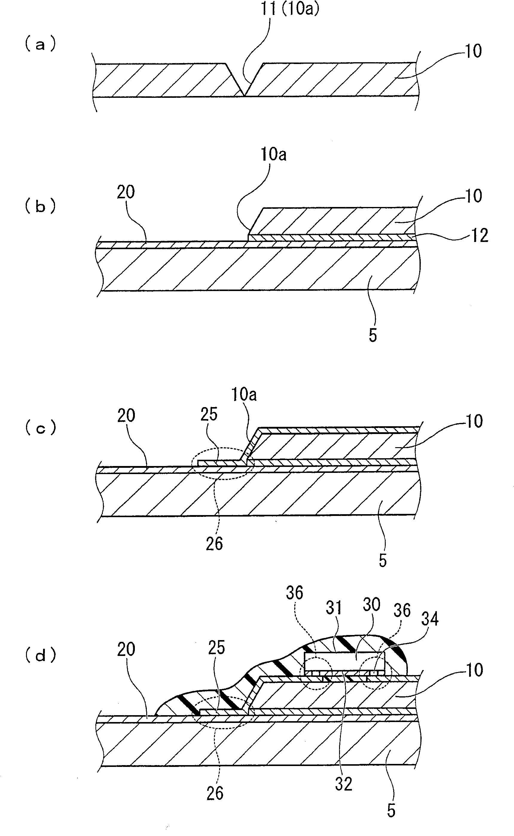
[0106] The first embodiment described above is different in that after the seed layer 13 is formed on the entire surface of the substrate 5 and the pedestal 10, plating is performed on the region (opening 15b) partitioned by the photoresist 15. processing, the second wiring 25 is formed. In contrast, in this embodiment, a silane coupling process is performed on a substrate to form a silane coupling film, a seed layer is formed on the silane coupling film, and a plating process is performed to form a second wiring. In addition, the basic configuration of other pattern forming methods is the same as that of the above-mentioned first embodiment, and the same symbols are assigned to common components, and detailed description thereof will be omitted.
[0107] Figure 5 (a)~(d) means along figure 2 The cross-sectional view taken along the line BB of the elect...
no. 3 approach
[0121] Next, a third embodiment of the electronic device of the present invention will be described.
[0122] Image 6 with Figure 7 It is a figure explaining the electronic device in 3rd Embodiment. Image 6 yes means Figure 7 The side sectional view of the C—C line looking down. Image 6 Symbol 2 in is an electronic device. Figure 7 It is a plan view that sees through a part of the electronic device 1 (resin 35 described later) from the vertical direction, and is a diagram for explaining the electronic device 2 of the present invention. In addition, the same code|symbol is attached|subjected to the component common to the said 1st Embodiment, and detailed description is abbreviate|omitted.
[0123] In the electronic device 2 of the present embodiment, the second wiring 25 of the electronic device 1 of the above-described embodiment covers and is connected to the electrode 34 . Here, the electrode 34 is formed on the electrode surface 32 of the IC chip 30, and is for...
PUM
 Abstract
Description
Claims
Application Information