Arrangement structure of electronic device and electronic circuit device

A technology of electronic devices and electronic circuits, which is applied in the field of configuration structures of electronic devices, can solve problems such as complicated procedures, difficult and cumbersome positioning of electronic devices, and achieve the effect of easy positioning

Active Publication Date: 2020-09-29
SHINDENGEN ELECTRIC MFG CO LTD
View PDF8 Cites 0 Cited by
  • Summary
  • Abstract
  • Description
  • Claims
  • Application Information

AI Technical Summary

Problems solved by technology

However, in this case, the positioning of the electronic device becomes difficult, and the process of arranging the electronic device on a flat surface becomes complicated and cumbersome

Method used


Image

  • Arrangement structure of electronic device and electronic circuit device
  • Arrangement structure of electronic device and electronic circuit device
  • Arrangement structure of electronic device and electronic circuit device

Examples


Embodiment Construction

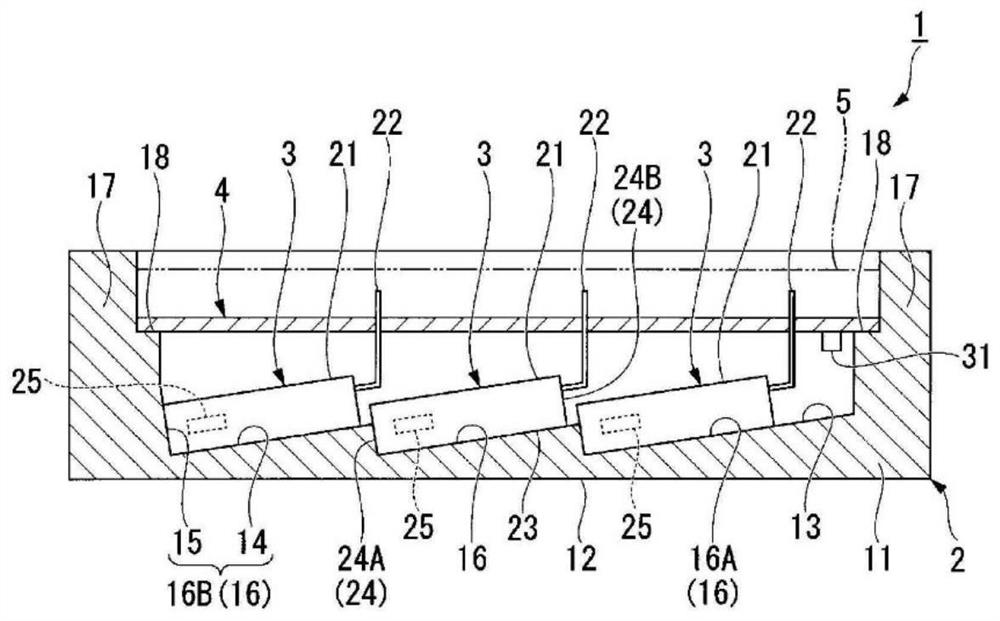
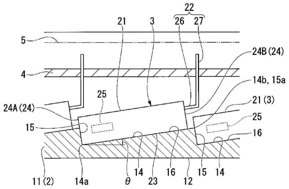
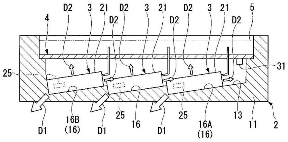
[0020] Below, will refer to Figure 1~5 One embodiment of the present invention will be described.

[0021] Such as figure 1 , 2 As shown, the arrangement structure of the electronic device and the electronic circuit device 1 in this embodiment include the base member 2 and the electronic device 3 . Furthermore, the electronic circuit device 1 of the present embodiment includes a substrate 4 electrically connected to the electronic device 3 .

[0022] The base material member 2 includes one formed in a plate shape, and in the thickness direction ( figure 1 , 2 The surface 12 on one side in the vertical direction) is the substrate main body 11 that is set as a flat surface. On the other surface 13 of the substrate main body 11 , an electronic device 3 to be described later is arranged.

[0023] exist figure 1 , 2 Among them, one side surface 12 of the substrate body 11 is a lower side facing downward. In addition, the surface 13 on the other side of the base body 11 is...


PUM


Abstract

Provided is an electronic device disposition structure comprising: a base member in which the surface on one side in the thickness direction thereof is a flat surface; and electronic devices that have a plate-shaped device body and are disposed on the surface on a second side of the base member. The surface on the second side includes: inclined surfaces inclined with respect to the surface on the one side; and rising surfaces rising from the lower end of the inclined surfaces. The electronic devices are disposed such that the main surfaces of the device bodies are in contact with the inclined surfaces, and the side surfaces of the device bodies come into contact with the rising surfaces.

Description

technical field [0001] The present invention relates to an arrangement structure of an electronic device and an electronic circuit device. Background technique [0002] Conventionally, when an electronic circuit device is constituted by a plurality of electronic devices (devices), it has been common practice to arrange the plurality of electronic devices on a single flat surface. [0003] Patent Document 1 discloses a configuration in which a plurality of drive ICs (electronic devices) that are rectangular in planar view are arranged side by side in one direction on the principal surface (single flat surface) of a substrate. , By inclining the long sides of a plurality of driving ICs in one direction, the driving ICs are mounted at a high density. [0004] 【Prior technical literature】 [0005] [Patent Document 1] Japanese Unexamined Patent Publication No. 5-254164 [0006] However, in the arrangement structure of the above-mentioned conventional electronic devices, since ...

Claims


Application Information

Patent Timeline
IPC IPC(8): H05K7/20H01L23/40
CPCH01L23/40H05K7/20
Inventor 岡野俊史
Owner SHINDENGEN ELECTRIC MFG CO LTD
Why Eureka
Try Eureka