Semiconductor substrate surface chemical processing method and apparatus

一种化学处理、基板表面的技术,应用在半导体基板进行化学处理,半导体基板进行湿化学处理领域,能够解决达不到要求、均一性差、增加镀膜和清洗膜的步骤等问题,达到增加距离、增大距离、杜绝可能性的效果

Active Publication Date: 2009-09-16
WUXI SUNTECH POWER CO LTD
View PDF5 Cites 0 Cited by
  • Summary
  • Abstract
  • Description
  • Claims
  • Application Information

AI Technical Summary

Problems solved by technology

However, the above-mentioned method of protecting with a mask and then performing wet chemical treatment also has great disadvantages: it not only increases the steps of coating and cleaning the film in the operation process, but also increases the cost of raw materials and the amount of wastewater generated during the treatment process.
In the above two cases, chemical treatment will be performed on the upper surface of the semiconductor substrate that does not need to be processed, so that the quality of the semiconductor substrate is unqualified or the uniformity is very poor, which cannot meet the requirements

Method used


Image

  • Semiconductor substrate surface chemical processing method and apparatus
  • Semiconductor substrate surface chemical processing method and apparatus
  • Semiconductor substrate surface chemical processing method and apparatus

Examples


specific Embodiment 1

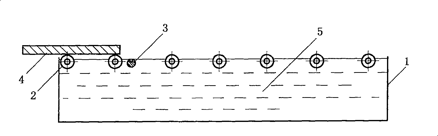
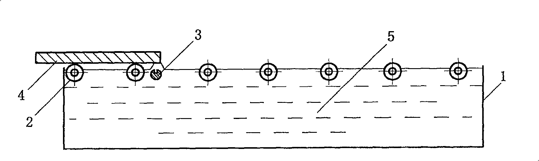
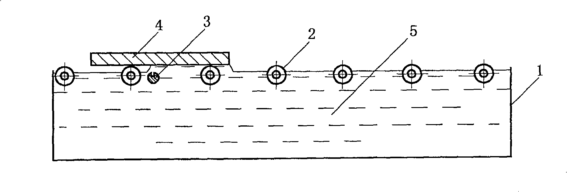
[0064] The chemical solution is a mixed solution of nitric acid and hydrofluoric acid. The injection device uses a nozzle and is fixed. The distance between the lower surface of the semiconductor substrate and the liquid surface of the chemical solution was 2 mm. When one edge of the semiconductor substrate moves over the nozzle, the nozzle sprays the chemical solution once. Then the lower surface of the semiconductor substrate is gradually wetted by the chemical solution under the action of surface tension as the semiconductor substrate continues to move. Throughout the process, the lower surface of the semiconductor substrate is in contact with the liquid level of the chemical solution in the chemical tank. After the treatment, the upper surface of the semiconductor substrate is not wetted by the chemical solution.

specific Embodiment 2

[0065]The injection device adopts multiple nozzles and is fixed. The distance between the lower surface of the semiconductor substrate and the liquid surface of the chemical solution was 10 mm. When one edge of the semiconductor substrate moves above the nozzle, the nozzle starts to spray the hydrofluoric acid solution until the other edge of the semiconductor substrate moves above the nozzle and stops. The semiconductor substrate continues to move, and when one edge of the semiconductor substrate moves above the next nozzle, the nozzle starts to spray the hydrofluoric acid solution until the other edge of the semiconductor substrate moves above the next nozzle and stops. During the whole process, the lower surface of the semiconductor substrate is not in contact with the liquid level of the chemical solution in the chemical bath. After the treatment, the upper surface of the semiconductor substrate is not wetted by the chemical solution.

specific Embodiment 3

[0066] The chemical solution is an electroless nickel plating solution. The injection device uses a nozzle and is fixed. The distance between the lower surface of the semiconductor substrate and the liquid surface of the chemical solution was 0.1 mm. When an edge of the semiconductor substrate moves above the nozzle, the nozzle starts to spray the electroless nickel plating solution. Continue until the other edge of the semiconductor substrate moves above the nozzle and stop. Throughout the process, the lower surface of the semiconductor substrate is in contact with the liquid level of the chemical solution in the chemical bath. After the treatment, the upper surface of the semiconductor substrate is not wetted by the chemical solution.


PUM


Abstract

The invention belongs to the field of semiconductor manufacturing industry. Specifically disclosed is a new chemical treatment method and device for the surface of a semiconductor substrate. In the chemical treatment method of the present invention, the semiconductor substrate is placed on the top of the chemical solution by using a bracket, and there is a certain distance between the lower surface of the semiconductor substrate and the liquid surface of the chemical solution, and the chemical solution is sprayed onto the lower surface of the semiconductor substrate by a spraying device. , so as to chemically treat the lower surface; wherein, the height of the chemical solution sprayed by the injection device is the distance between the lower surface of the semiconductor substrate and the upper port of the injection device. The device of the present invention includes a chemical tank containing a chemical solution, a support for placing a semiconductor substrate above the chemical solution, and a spraying device for spraying the chemical solution onto the lower surface of the semiconductor substrate. The chemical treatment method and its device of the present invention can only perform chemical treatment on a certain surface of the semiconductor substrate without any protection on the other surface.

Description

technical field [0001] The present invention relates to a technology for chemically treating a semiconductor substrate in the semiconductor manufacturing industry, in particular to a method for performing wet chemical treatment on a semiconductor substrate in the field of preparing semiconductor solar cells; more specifically, it involves performing wet chemical treatment on a certain surface of a semiconductor substrate The method of processing. Background technique [0002] Treating the surface of a semiconductor substrate with a chemical solution is a common process in the semiconductor manufacturing industry. For example, a surface etching process and a cleaning process are performed on the semiconductor substrate. Generally, the above wet chemical treatment process is carried out by immersing the semiconductor substrate in a chemical solution. In this case, wet chemical treatment is performed on both surfaces of the semiconductor substrate. [0003] However, in the i...

Claims


Application Information

Patent Timeline
Patent Type & Authority Patents(China)
IPC IPC(8): H01L21/306C23F1/24
CPCH01L21/67086H01L21/30604H01L21/67057H01L21/302H01L21/306
Inventor 季静佳覃榆森施正荣
Owner WUXI SUNTECH POWER CO LTD
Why Eureka
Try Eureka