

Defects detection device and method
A defect inspection and defect technology, which is applied in the direction of optical test defect/defect, semiconductor/solid-state device test/measurement, etc., can solve the problem that the defect image cannot be directly confirmed, and achieve the effect of suppressing vibration
- Summary
- Abstract
- Description
- Claims
- Application Information
AI Technical Summary
Problems solved by technology
Method used
Image

Examples
Embodiment Construction
[0032] Hereinafter, embodiments of the present invention will be described with reference to the drawings.
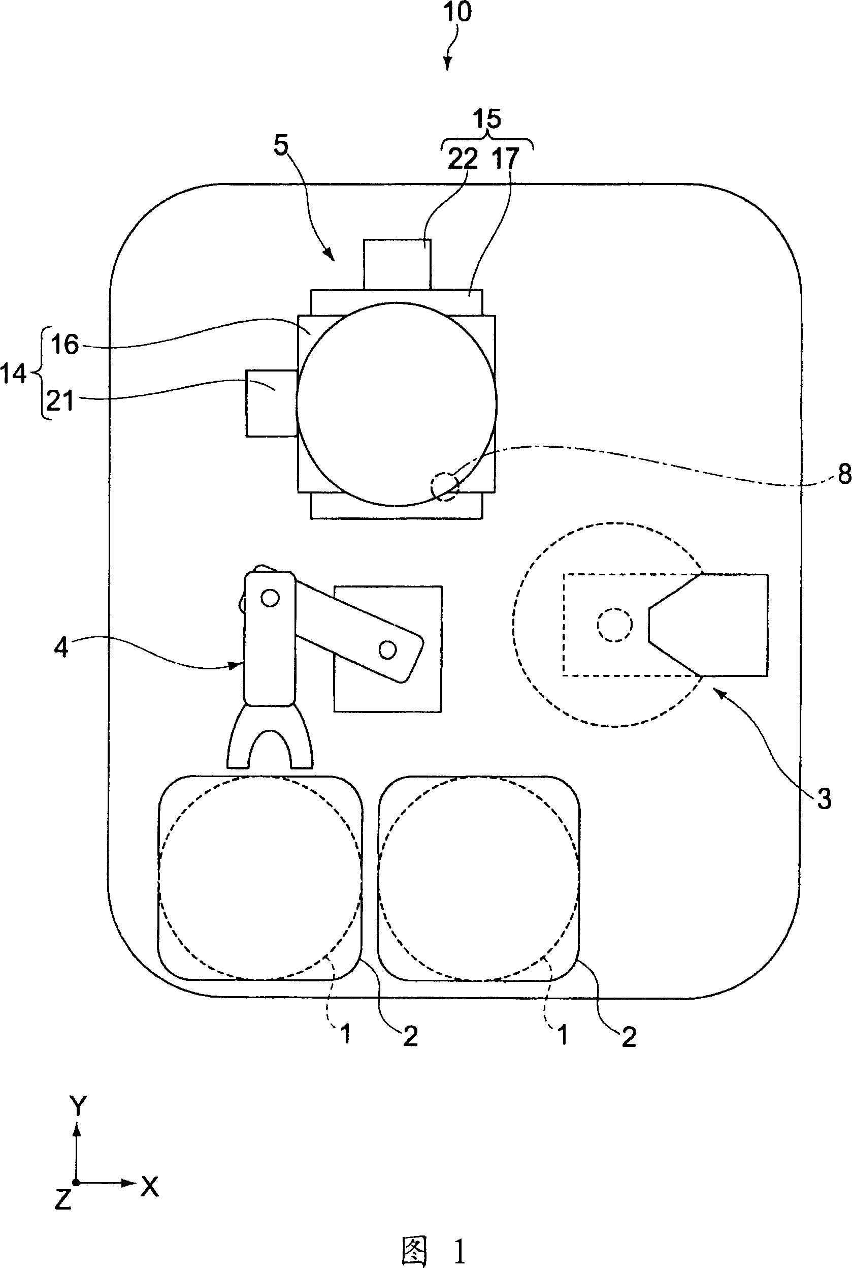
[0033] FIG. 1 is a schematic plan view showing a defect inspection device according to an embodiment of the present invention.
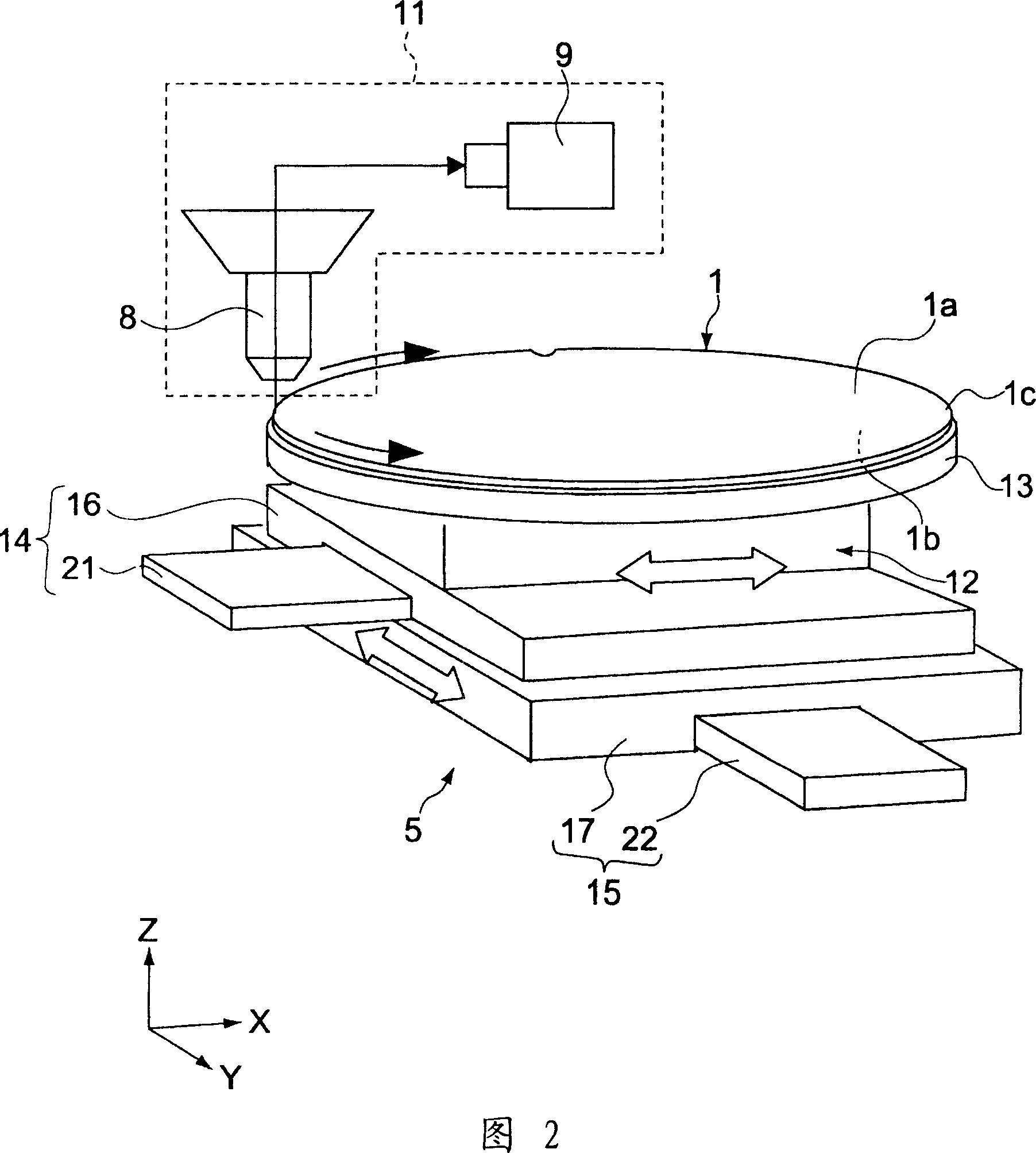
[0034] The defect inspection apparatus 10 includes: a cassette 2 for accommodating a semiconductor wafer substrate 1 (hereinafter simply referred to as a wafer); a pre-positioner 3; an XY moving mechanism 5; a transfer robot 4; and an imaging device 11 (see FIG. 2 ). The transfer robot 4 transfers the wafer 1 between the cassette 2 , the pre-positioner 3 and the XY moving mechanism 5 . The pre-positioner 3 roughly adjusts (pre-positions) the in-plane rotation angle of the wafer 1 transferred from the transfer robot 4 .
[0035] The defect inspection apparatus 10 handles wafers 1 of, for example, 8 inches and 12 inches, but wafers 1 of sizes other than the above-mentioned sizes can also be handled. The box 2 may be either an open type or a cl...
PUM
 Abstract
Description
Claims
Application Information