Supercharge Your Innovation With Domain-Expert AI Agents!

Plane display and display driving method

A display driving and display technology, which is applied to static indicators, cathode ray tube indicators, instruments, etc., can solve the problems of affecting the yield of flat-panel displays, high impedance of signal lines, increasing the weight of flat-panel displays 100, and manufacturing costs.

Inactive Publication Date: 2007-08-01
INNOLUX CORP
View PDF0 Cites 2 Cited by
  • Summary
  • Abstract
  • Description
  • Claims
  • Application Information

AI Technical Summary

Problems solved by technology

[0004] However, since this Chip On Glass (COG) transmission architecture must use multiple flexible circuit boards 130 to transmit RSDS signals, the weight and manufacturing cost of the entire flat panel display 100 are increased.
In addition, if the wire on array (WOA) transmission architecture is used to reduce the weight and cost of the flat panel display, the transmission lines between the data drivers are directly arranged on the glass substrate to transmit the RSDS signal, and the impedance of the signal line will be too large. The problem seriously affects the yield of flat panel displays

Method used


Image

  • Plane display and display driving method
  • Plane display and display driving method
  • Plane display and display driving method

Examples


Embodiment Construction

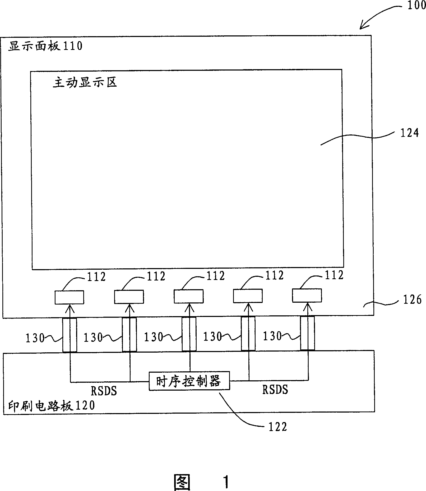
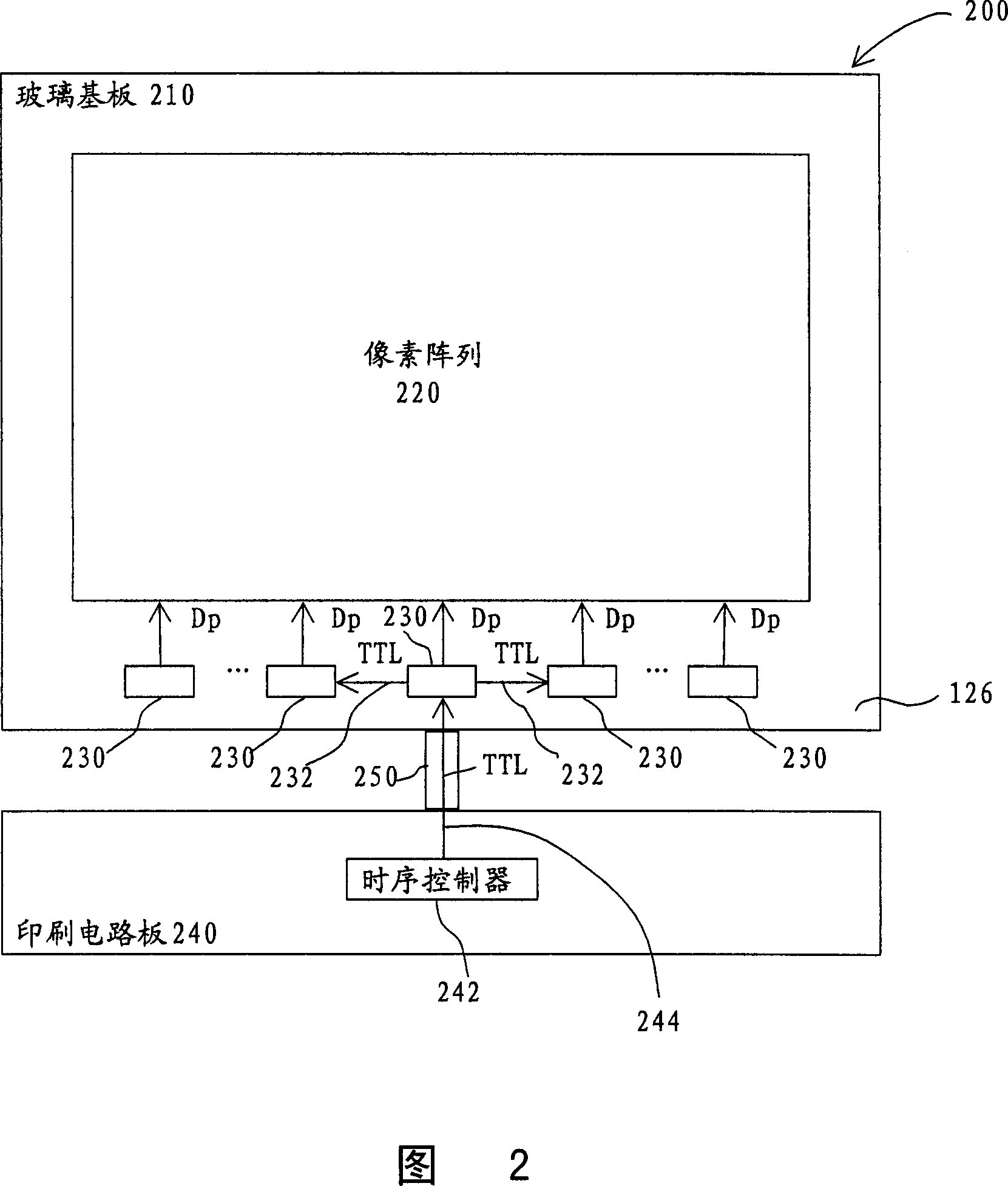
[0073] The flat panel display in the following embodiments, such as a liquid crystal display, is used for the timing controller to transmit the pixel data to the specified data driver, and then the specified data driver transmits the pixel data to other data drivers.

[0074] Please refer to FIG. 2 , which shows a structural block diagram of a flat panel display according to a preferred embodiment of the present invention. The flat panel display 200 , such as a liquid crystal display, includes a glass substrate 210 , a pixel matrix 220 , a data driver 230 and a printed circuit board 240 . The pixel array 220 includes arrayed pixel circuits disposed on the glass substrate 210 for displaying images. The data driver 230 is disposed on the glass substrate 210 using gold contact bump technology (described later). The transmission lines 232 between the data drivers are directly disposed on the glass substrate 210 in a WOA transmission structure. The data driver 230 outputs the pix...


PUM


Abstract

This invention discloses one display device, which comprises one array pixel circuit and multiple data drivers to drive pixel circuit, wherein, the data driver comprises one first data driver and second data driver; the first driver is to receive pixel data according to first clock impulse frequency and to send the pixel data to second driver according to second impulse frequency with different frequency to first one.

Description

technical field [0001] The present invention relates to a flat display, in particular to a flat display using a transistor-to-transistor logic (Transistor to Transistor Logic, TTL) transmission mode, and a display driving method. Background technique [0002] FIG. 1 shows a flat panel display 100 including a display panel 110 and a printed circuit board 120 . The display panel 110 has an active display area 124 , and the active display area 124 has an array of pixel circuits for displaying pixel images. Each pixel includes, for example, a red sub-pixel, a green sub-pixel and a blue sub-pixel, and each pixel circuit corresponds to a sub-pixel. The pixel circuits are driven by corresponding data drivers 112 . The pixel circuit is disposed on the glass substrate 126 , and the data driver 112 is disposed outside the active display area 124 adjacent to the edge of the glass substrate 126 . The printed circuit board 120 includes a timing controller 122 for transmitting pixel da...

Claims


Application Information

Patent Timeline
Patent Type & Authority Applications(China)
IPC IPC(8): G09G3/20G09G5/00G09G5/02G09F9/30
Inventor 辜宗尧蔡永裕
Owner INNOLUX CORP
Features
  • R&D
  • Intellectual Property
  • Life Sciences
  • Materials
  • Tech Scout
  • Unparalleled Data Quality
  • Higher Quality Content
  • 60% Fewer Hallucinations
Learn More