Base semiconductor chip, semiconductor integrated circuit device, and semiconductor integrated circuit device manufacturing method

A technology of integrated circuit and manufacturing method, which is applied in the direction of semiconductor/solid-state device manufacturing, semiconductor devices, semiconductor/solid-state device components, etc., can solve the problems of inseparable interconnection test function blocks and difficult identification of test function blocks, etc., to prevent Increase in inventory, prevent increase in power consumption, and shorten the period of time

Inactive Publication Date: 2007-08-01
PANASONIC CORP
View PDF2 Cites 0 Cited by
  • Summary
  • Abstract
  • Description
  • Claims
  • Application Information

AI Technical Summary

Problems solved by technology

However, it is difficult to identify the test function block and it is not possible to separate the interconnected test function blocks after testing

Method used


Image

  • Base semiconductor chip, semiconductor integrated circuit device, and semiconductor integrated circuit device manufacturing method
  • Base semiconductor chip, semiconductor integrated circuit device, and semiconductor integrated circuit device manufacturing method
  • Base semiconductor chip, semiconductor integrated circuit device, and semiconductor integrated circuit device manufacturing method

Examples


Embodiment 1

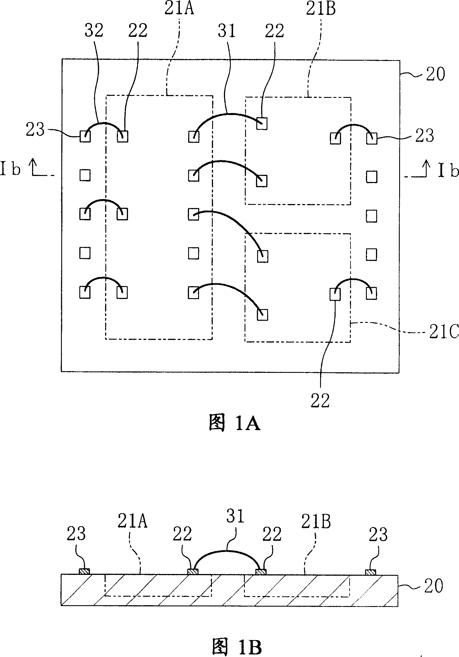
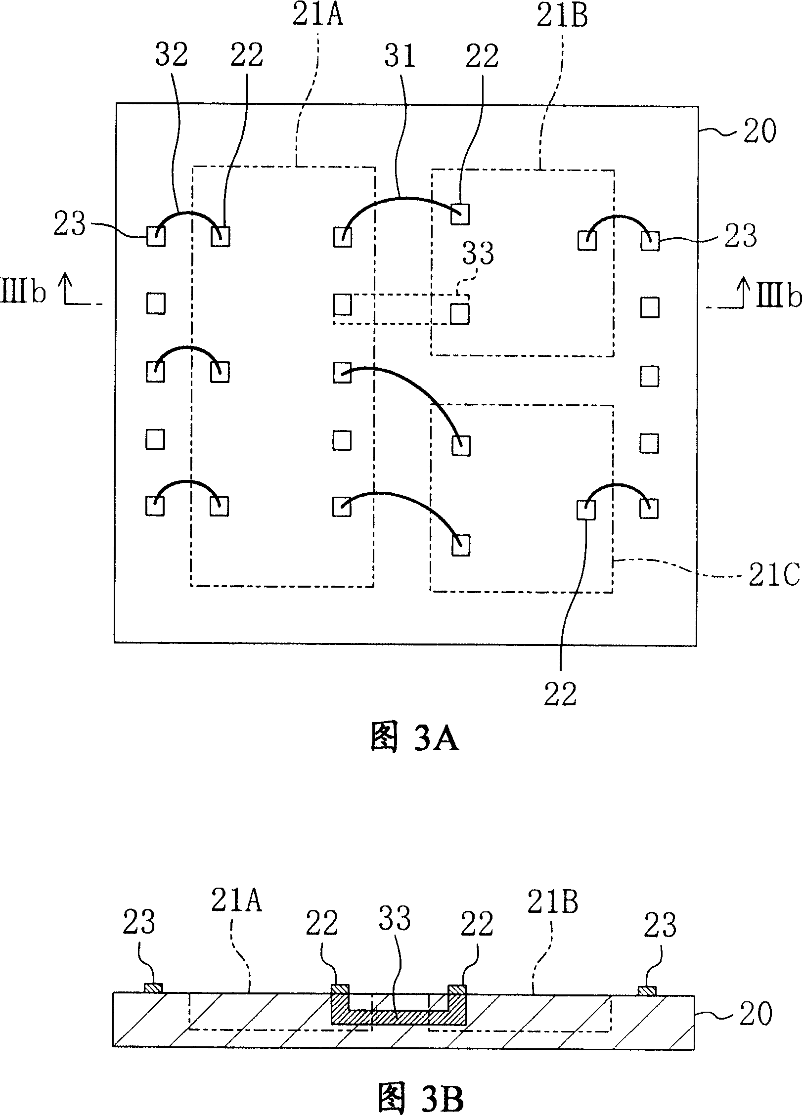
[0054] Embodiment 1 of the present invention will be described with reference to the drawings. 1 shows a main part of a semiconductor integrated circuit device (LSI circuit) according to Embodiment 1, wherein FIG. 1A is a plan view, and FIG. 1B is a cross-sectional view taken along line Ib-Ib in FIG. 1A.

[0055] As shown in FIG. 1, the LSI circuit of the present embodiment includes: a basic semiconductor chip 20 as a semiconductor substrate in which a plurality of functional blocks as a semiconductor integrated circuit are formed; and interconnections for interconnecting the functional blocks. Even 31. In FIG. 1 , three functional blocks of a first functional block 21A, a second functional block 21B, and a third functional block 21C are provided as an example. Each functional block may be any functional block such as a microprocessor, memory or the like.

[0056] These functional blocks are formed independently of each other in a predetermined region of the base semiconduct...

Embodiment 2

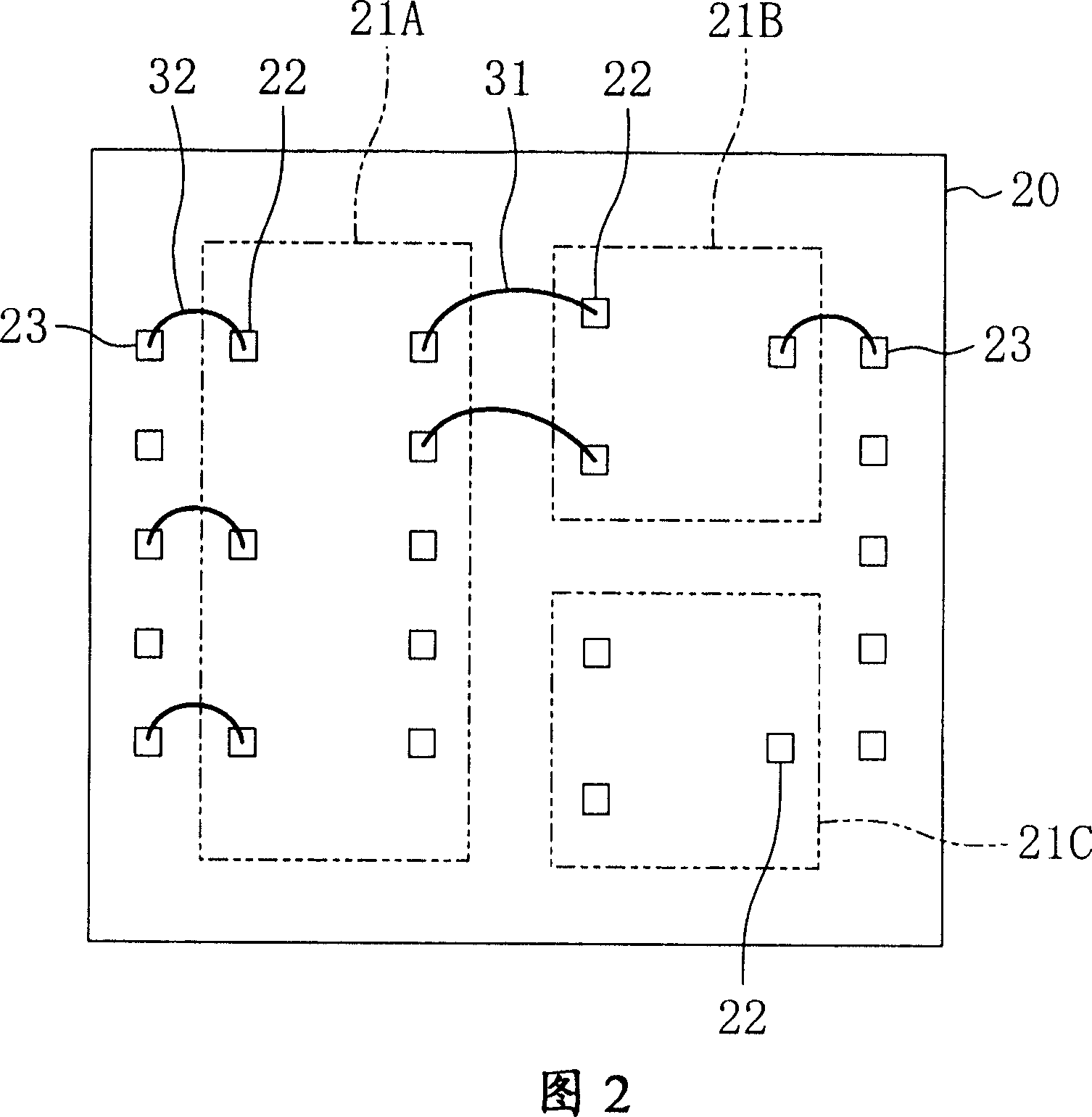
[0073] Embodiment 2 of the present invention will be described below with reference to the drawings. FIG. 10 shows a basic semiconductor chip 40 according to Embodiment 2. As shown in FIG. In Embodiment 2, a portion including necessary functional blocks is cut out from a base semiconductor chip to form an LSI circuit including necessary functions.

[0074] As shown in FIG. 10, the basic semiconductor chip 40 is composed of a plurality of functional blocks formed in a semiconductor substrate. For example, the basic semiconductor chip 40 shown in FIG. 10 includes six functional blocks: a first functional block 21A, a second functional block 21B, a third functional block 21C, a fourth functional block 21D, a fifth functional block 21E, and a sixth functional block. Function block 21F.

[0075] Although not shown, similarly to FIG. 1 , a plurality of functional block pads 22 are formed along the periphery of the functional block. Therefore, each region forming a functional bloc...


PUM


Abstract

A semiconductor integrated circuit device includes: a semiconductor substrate; a semiconductor chip including a plurality of functional blocks formed independently from each other in predetermined regions of the semiconductor substrate and each including a pad for transmitting a signal; and a plurality of inter-pad interconnects being connected to the pads and being capable of being cut. Signal transmission between the respective functional blocks is performed through the respective inter-pad interconnects.

Description

technical field [0001] The present invention relates to a basic semiconductor chip, a semiconductor integrated circuit device using the same, and a method of manufacturing the semiconductor integrated circuit device, wherein the basic semiconductor chip includes a semiconductor substrate in which a plurality of functional blocks are formed. Background technique [0002] As is well known, a multi-chip module (MCM) is one of semiconductor chips having complex processing functions, in which a plurality of semiconductor chips including a semiconductor integrated circuit are arranged on a die pad and packaged (see, for example, Japan Patent Application Publication No. 2000-349226A (FIG. 1)). [0003] However, for the MCM, it is necessary to prepare a plurality of semiconductor chips having different functions, to determine the layout of the semiconductor chips on the die pad, and to interconnect the chips with wiring or the like and to interconnect the chip with the die pad. eve...

Claims


Application Information

Patent Timeline
Patent Type & Authority Applications(China)
IPC IPC(8): H01L27/04H01L23/52H01L21/822H01L21/768
CPCH01L2224/48091H01L24/18H01L2224/24137H01L2224/48137H01L2224/05553H01L2924/14H01L2224/4813H01L2224/18H01L2924/00014H01L2924/00H01L2924/00012
Inventor 石山裕浩
Owner PANASONIC CORP
Why Eureka
Try Eureka