
Bias circuits

A bias circuit and circuit technology, applied in the direction of adjusting electrical variables, instruments, control/regulation systems, etc., can solve the problems of bandgap reference and temperature sensor initial accuracy degradation, influence propagation and temperature dependence, etc.

Active Publication Date: 2007-08-22
VLSI TECH LLC
View PDF0 Cites 13 Cited by
  • Summary
  • Abstract
  • Description
  • Claims
  • Application Information

AI Technical Summary

Problems solved by technology

Therefore, regarding B F The dependence of V BE The propagation and temperature dependence of , and will become more severe with each new process production, degrading the initial accuracy of bandgap references and temperature sensors

Method used


Image

  • Bias circuits
  • Bias circuits
  • Bias circuits

Examples


Embodiment Construction

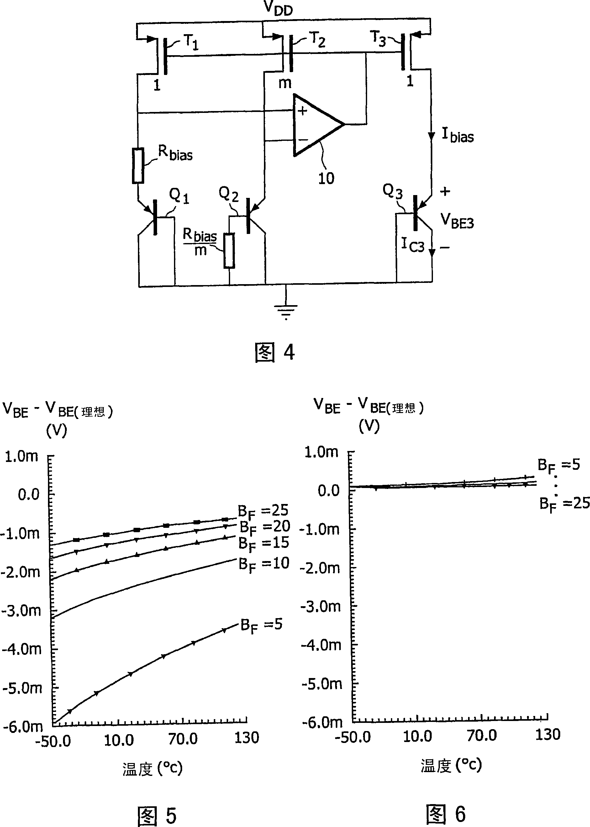
[0033] A circuit diagram of a bias circuit embodying the present invention is shown in FIG. 4 . Utilizing an additional resistor R connected in series with the base of Q2 bias / m, given by the equation for bias current I bias expression for:

[0034] V BE 1 + I bias R bias = m I bias 1 I + B F R bias m + V BE 2

[0035] ⇒ I bias = 1 + B F B ...


PUM


Abstract

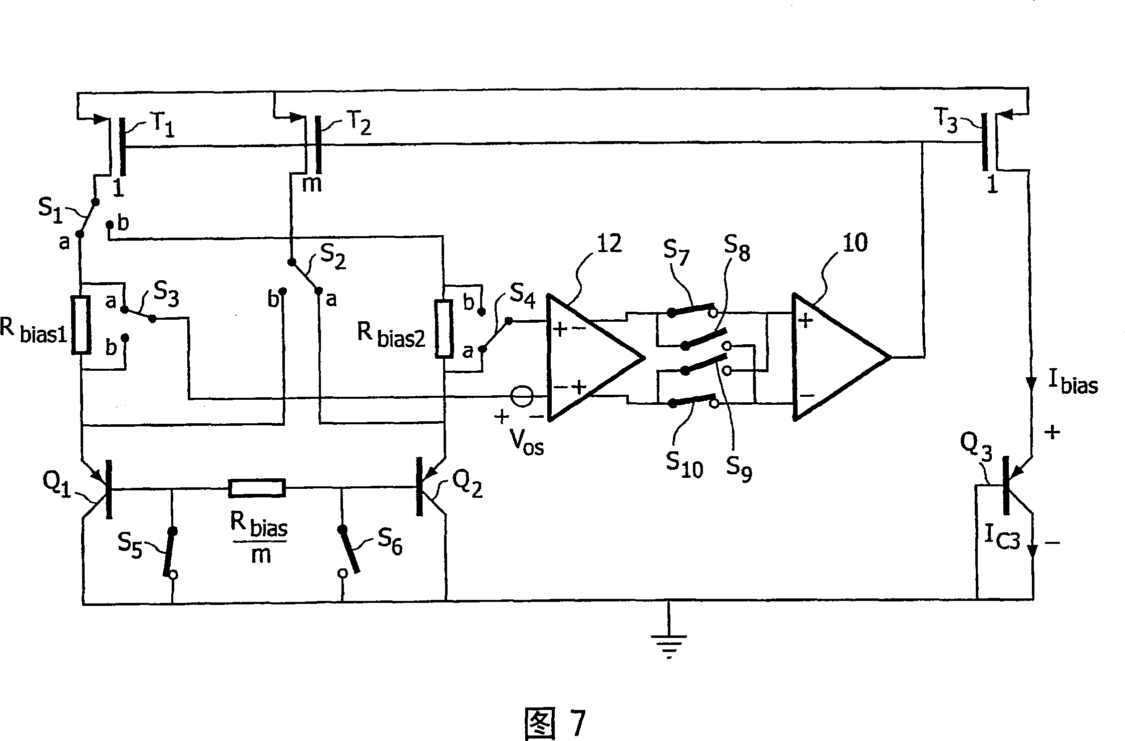
The invention provides a bandgap voltage reference circuit and a bias circuit in a temperature probe, which comprises a pair of transistors (Q1, Q2). The first transistor (Q1) of the transistors (Q1, Q2) is biased with emitter current Ibias, and the second transistor is biased with the current of m times of the emitter current mIbias. The circuit is set so that difference of the base-emitter voltage of the transistor is partially produced on both ends of a first resistor device of Rbias used for carrying bias current equal to Ibias, and difference of the base-emitter voltage of the transistor is partially produced on both ends of a second resistor with the resistance substantially equal to Rbias / m and used for carrying the current equal to the base current of the second transistor. Resultantly, when an emitter through a liner bipolar transistor biases the lining bipolar transistor, the bias current Ibias which is substantially the collected current of PTAT produced therefrom, and the base-emitter voltage substantially independent of the forward current gain of the liner bipolar transistor are used.

Description

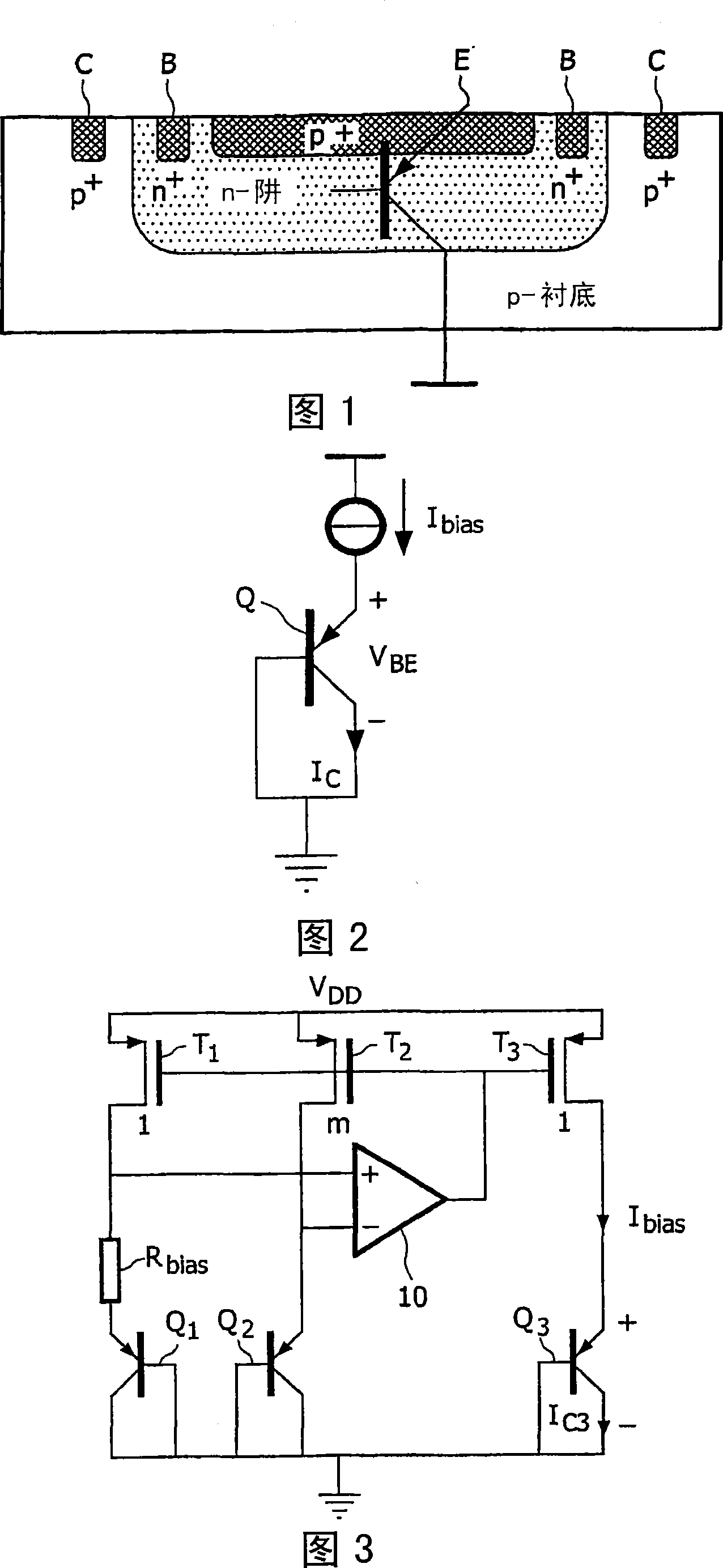
technical field [0001] The present invention relates to a bias circuit, and more particularly, to a bias circuit for use in, for example, bandgap voltage reference circuits and temperature sensors. Background technique [0002] Bias circuits that generate a current proportional to absolute temperature (PTAT) are widely used in integrated circuits. Their main application is in temperature-independent biasing in bipolar transistors (and CMOS transistors in weak-inversion). PTAT biasing circuits are also used in bandgap voltage references, where the PTAT voltage is combined with the base-emitter voltage of a bipolar transistor to produce a temperature-independent reference voltage. Another application is in temperature sensors, where PTAT voltage or current is used as a measure of temperature. [0003] PTAT bias circuits, bandgap references, and temperature sensors in CMOS technology are often based on substrate bipolar transistors (Figure 1). The collector of such a transis...

Claims


Application Information

Patent Timeline
Patent Type & Authority Applications(China)
IPC IPC(8): G05F3/20
Inventor 迈克尔·A·P·佩尔蒂斯约翰·H·胡声
Owner VLSI TECH LLC
Learn More