
Lateral double-diffused mosfet (LDMOS) transistor and a method of fabricating the same

A technology of transistors and oxide layers, applied in semiconductor/solid-state device manufacturing, transistors, semiconductor devices, etc., can solve problems such as incompatibility

Active Publication Date: 2010-12-08
VOLTERRA SEMICONDUCTOR
View PDF3 Cites 2 Cited by
  • Summary
  • Abstract
  • Description
  • Claims
  • Application Information

AI Technical Summary

Problems solved by technology

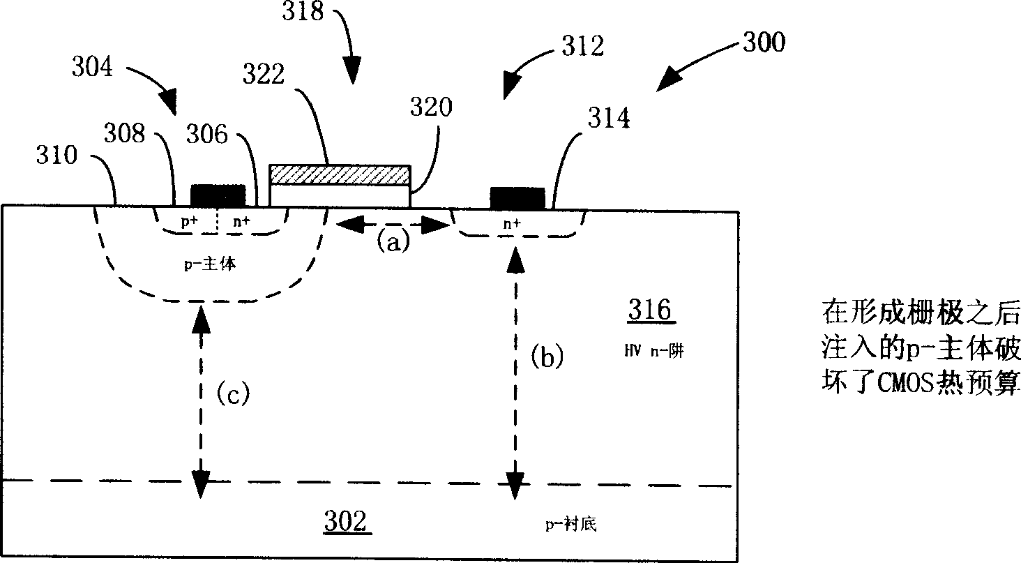
However, the BCD process includes the growth of the HV n-Epi layer 346, and this step is generally not compatible with sub-micron CMOS processes

Method used


Image

  • Lateral double-diffused mosfet (LDMOS) transistor and a method of fabricating the same
  • Lateral double-diffused mosfet (LDMOS) transistor and a method of fabricating the same
  • Lateral double-diffused mosfet (LDMOS) transistor and a method of fabricating the same

Examples


Embodiment Construction

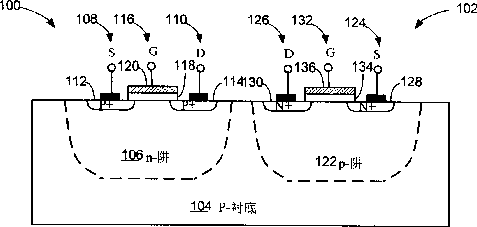
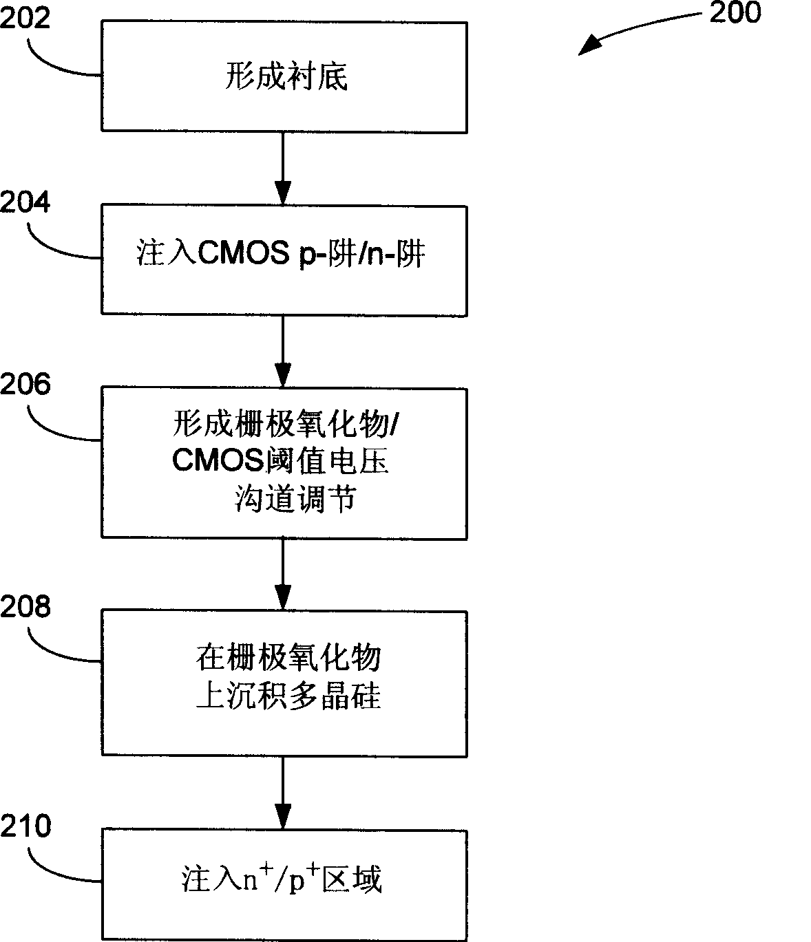
[0045] Figure 4 Shown is a block diagram of a switching regulator including LDMOS transistors according to one embodiment. Conventional LDMOS transistors typically achieve optimized device performance through complex processes such as BiCMOS processes or BCD processes that include one or more process steps that are incompatible with sub-micron processes for mass-produced digital sub-micron CMOS transistors . According to one aspect, there is provided an LDMOS transistor fabricated by a process fully integrated into a typical sub-micron CMOS process.

[0046] refer to Figure 4 , the exemplary switching regulator 400 is connected to a first high DC input voltage source 402 such as a battery through an input terminal 404 . The switching regulator 400 is also connected to a load 406 such as an integrated circuit through an output terminal 408 . The switching regulator 400 acts as a direct current to direct current (DC-to-DC) converter between an input terminal 404 and an out...


PUM


Abstract

Methods and systems for monolithically fabricating a lateral double-diffused MOSFET (LDMOS) transistor having a source, drain, and a gate on a substrate, with a process flow that is compatible with a CMOS process flow are described.

Description

technical field [0001] The present invention relates to a semiconductor device. Background technique [0002] Voltage regulators such as DC to DC converters are used to provide a stable voltage source for electronic systems. Efficient DC-to-DC converters are especially needed for battery management in low power devices such as laptops and cell phones. Known switching voltage regulators (or simply "switching regulators") are a class of efficient DC-to-DC converters. A switching regulator generates an output DC voltage by converting an input DC voltage to a high-frequency voltage and filtering the high-frequency input voltage. In particular, switching regulators include switches for selectively coupling and decoupling an input DC voltage source, such as a battery, to a load, such as an integrated circuit. An output filter, typically comprising an inductor and a capacitor, is coupled between the input voltage source and the load to filter the output of the switch and thus pr...

Claims


Application Information

Patent Timeline
Patent Type & Authority Patents(China)
IPC IPC(8): H01L21/336H01L29/78
CPCH01L27/088H01L29/1095H01L29/42368H01L29/7816H01L29/7835H01L21/823814H01L29/086H01L29/0696H01L21/823892H01L29/6625H01L29/66689H01L27/0922H01L29/0878
Inventor 游步东马可·A·苏尼加
Owner VOLTERRA SEMICONDUCTOR
Learn More